Method for making organic light emitting diode

a light-emitting diode and organic technology, applied in the direction of electrical equipment, semiconductor devices, solid-state devices, etc., can solve the problems of poor dispersion of carbon nanotubes in melted polymer, and affecting the uniformity of carbon nanotubes in composite structures

Active Publication Date: 2019-02-28
TSINGHUA UNIV +1
View PDF3 Cites 3 Cited by
  • Summary
  • Abstract
  • Description
  • Claims
  • Application Information

AI Technical Summary

Benefits of technology

[0004]The carbon nanotube composite structure formed by carbon nanotubes and polymer can be used as the electron transport layer of the OLED. The carbon nanotube composite structure can be formed by two methods. One method includes dispersing the carbon nanotubes into an organic solvent to form a carbon nanotube dispersion, mixing the carbon nanotube dispersion and a monomer solution, and polymerizing the monomer. However, the carbon nanotubes have poor dispersion in the organic solvent, which affects the uniformity of the carbon nanotubes in the composite structure. Another method include completely melting the polymer, and mixing the melted polymer and the carbon nanotubes. However, the carbon nanotubes have poor dispersion in the melted polymer because the melted polymer has greater viscosity. Thus, the uniformity of the carbon nanotubes in the composite structure is still poor. When the carbon nanotube composite structure is used as the electron transport layer of the OLED, the electron transport layer has poor ability to transmit electrons.

Problems solved by technology

However, the carbon nanotubes have poor dispersion in the organic solvent, which affects the uniformity of the carbon nanotubes in the composite structure.
However, the carbon nanotubes have poor dispersion in the melted polymer because the melted polymer has greater viscosity.
Thus, the uniformity of the carbon nanotubes in the composite structure is still poor.
When the carbon nanotube composite structure is used as the electron transport layer of the OLED, the electron transport layer has poor ability to transmit electrons.

Method used


Image

  • Method for making organic light emitting diode
  • Method for making organic light emitting diode
  • Method for making organic light emitting diode

Examples


first embodiment

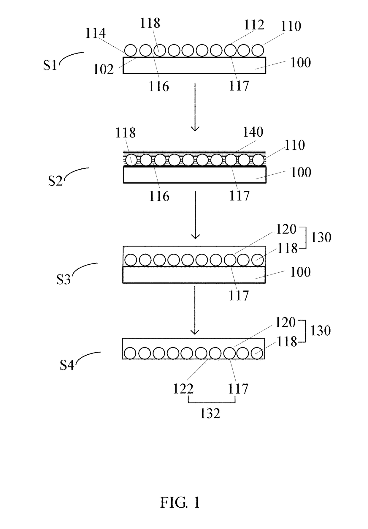
[0045]Referring to FIG. 1, a method for making a carbon nanotube composite structure 130 of a first embodiment includes the following steps:

[0046]S1, placing a carbon nanotube structure 110 on a substrate surface 102 of a substrate 100, wherein the carbon nanotube structure 110 has a first surface 112 and a second surface 114 opposite to the first surface 112, and the second surface 114 is in direct contact with the substrate surface 102;

[0047]S2, coating a monomer solution 140 on the carbon nanotube structure 110, wherein the monomer solution 140 is formed by dispersing a certain amount of monomers into an organic solvent;

[0048]S3, polymerizing the monomer; and

[0049]S4, removing the substrate 100.

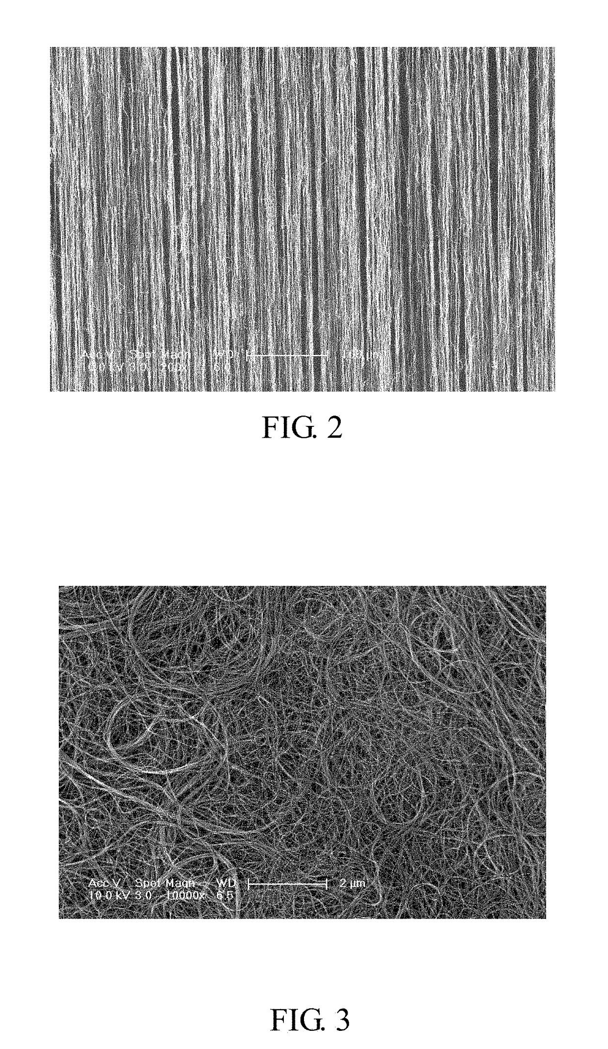
[0050]In the step S1, the carbon nanotube structure 110 includes a plurality of carbon nanotubes 118 uniformly distributed therein. A gap 116 is defined between adjacent carbon nanotubes 118. The plurality of carbon nanotubes 118 is parallel to the first surface 112 and the second surface ...

second embodiment

[0069]Referring to FIG. 10, a method for making a carbon nanotube composite structure 160 of a second embodiment includes the following steps:

[0070]S21, placing the carbon nanotube structure 110 on the substrate surface 102 of the substrate 100, wherein the carbon nanotube structure 110 has the first surface 112 and the second surface 114 opposite to the first surface 112, and the second surface 114 is in direct contact with the substrate surface 102;

[0071]S22, locating a graphene layer 150 on the first surface 112;

[0072]S23, coating a monomer solution 140 on the graphene layer 150 and the carbon nanotube structure 110, wherein the monomer solution 140 is formed by dispersing the monomer into the organic solvent;

[0073]S24, polymerizing the monomer; and

[0074]S25, removing the substrate 100.

[0075]In this embodiment, the method for making the carbon nanotube composite structure 160 is similar to the method for making the carbon nanotube composite structure 130 above except that the gra...

third embodiment

[0077]Referring to FIG. 11, a method for making a carbon nanotube composite structure 170 of a third embodiment includes the following steps:

[0078]S31, placing the carbon nanotube structure 110 on the substrate surface 102 of the substrate 100 to form a preform structure 172, wherein the carbon nanotube structure 110 has the first surface 112 and the second surface 114 opposite to the first surface 112, and the second surface 114 is in direct contact with the substrate surface 102;

[0079]S32, locating two preform structures 172 on a base 174, wherein the two preform structures 172 are spaced apart from each other, the substrates 100 of the two preform structures 172 and the base 174 form a mold 176 having an opening, and the carbon nanotube structures 110 of the two preform structures 172 are opposite to each other and inside of the mold 176;

[0080]S33, injecting the monomer solution 140 into the inside of the mold 176 from the opening of the mold 176, wherein the monomer solution 140...


PUM

PropertyMeasurementUnit
angleaaaaaaaaaa
diameteraaaaaaaaaa
diameteraaaaaaaaaa

Abstract

A method for making an organic light emitting diode includes providing a preform structure including an anode electrode, a hole transport layer, and an organic light emitting layer stacked on each other in that order. A carbon nanotube composite structure including a polymer and a plurality of first carbon nanotubes dispersed in the polymer is also provided. The plurality of first carbon nanotubes is substantially parallel to each other, and a part of surface of the plurality of first carbon nanotubes is exposed from the polymer. The preform structure, the carbon nanotube composite structure and a cathode electrode are stacked on each other in that order.

Description

CROSS-REFERENCE TO RELATED APPLICATIONS[0001]This application claims all benefits accruing under 35 U.S.C. § 119 from China Patent Application No. 201710766482.5, filed on Aug. 30, 2017, in the China Intellectual Property Office. This application is related to commonly-assigned application entitled, “ORGANIC LIGHT EMITTING DIODE”, concurrently filed (Atty. Docket No. US71645); “ORGANIC LIGHT EMITTING DIODE”, concurrently filed (Atty. Docket No. US71646); “ORGANIC LIGHT EMITTING DIODE”, concurrently filed (Atty. Docket No. US71647); “METHOD FOR MAKING ORGANIC LIGHT EMITTING DIODE”, concurrently filed (Atty. Docket No. US71648); “METHOD FOR MAKING ORGANIC LIGHT EMITTING DIODE”, concurrently filed (Atty. Docket No. US71649); “METHOD FOR MAKING ORGANIC LIGHT EMITTING DIODE”, concurrently filed (Atty. Docket No. US71650). Disclosures of the above-identified applications are incorporated herein by reference.FIELD[0002]The present application relates to organic light emitting diodes and me...

Claims


Application Information

Patent Timeline
Patent Type & Authority Applications(United States)
IPC IPC(8): H01L51/50H01L51/56H01L51/00
CPCH01L51/5072H01L51/56H01L51/0035H01L51/0048H01L51/003H01L51/0024H01L51/0003H01L51/0012H10K85/221H10K50/16H10K71/00H10K71/191H10K85/111H10K71/12H10K71/50H10K71/80
Inventor NING, WENLIU, PENGJIANG, KAI-LIFAN, SHOU-SHAN
Owner TSINGHUA UNIV
Why Eureka
Try Eureka