Liquid crystal display and production method therefor

Active Publication Date: 2019-03-14
SHARP KK
View PDF3 Cites 1 Cited by
  • Summary
  • Abstract
  • Description
  • Claims
  • Application Information

AI Technical Summary

Benefits of technology

The present technology is about a new liquid crystal display and a method of producing it. It is designed to have a high contrast while maintaining good display reliability. The technology involves using an alignment film and an alignment-controlling layer to increase the contrast and align the liquid crystal material. By subjecting one substrate to a high temperature treatment and treating it with rubbing or light irradiation, the alignment film improves the contrast. The absence of an alignment film on another substrate avoids various defects that could occur during the formation of the alignment film. Overall, this technology produces a liquid crystal display that has excellent display reliability and high contrast.

Problems solved by technology

However, not only are many steps necessary for forming the alignment film but also issues, such as coating irregularity and dust generation caused by the rubbing or alignment treatment, occur.
However, an aperture ratio may be decreased or light may leak out by the structure for regulating alignment.
According to the alignment film-less liquid crystal alignment technology described above, the alignment treatment using the rubbing cannot be performed and it is necessary to control the alignment of the liquid crystal only by the material design of the liquid crystal composition.
It is difficult, accordingly, to sufficiently align the liquid crystals, and the increase of the contrast is a problem to be solved.
On the other hand, according to the structure in which the conventional alignment films are provided on the two substrates as the conventional PSA technology, the high contrast can be expressed, but various defects caused by the formation of the alignment film cannot be avoided.
The defects caused by the formation of the alignment film may include, in the array substrate, electrical connection failure and occurrence of uneven alignment, caused by difficulty in precise control of an area on which the alignment film is formed, increased moisture absorbency due to thermal denaturation of a material for forming an insulating film, and the like; and in the counter substrate, thermal decomposition and elution of a color material of a color filter layer, thermal deviation of retardation (phase difference) of an intracellular phase difference layer, and the like.
All of them reduce display reliability of a liquid crystal display.

Method used


Image

  • Liquid crystal display and production method therefor
  • Liquid crystal display and production method therefor
  • Liquid crystal display and production method therefor

Examples


first embodiment

isplay Including Array Substrate Having NQD-Containing Organic Insulating Film but Having No Alignment Film, and Counter Substrate Having Alignment Film

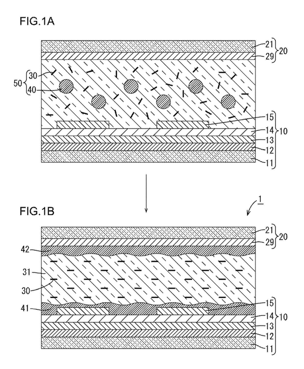
[0025]A first embodiment is explained using FIGS. 1A and 1B. The present first embodiment exemplifies a liquid crystal display including an array substrate 10 having an NQD-containing organic insulating film 12. In the present first embodiment, a counter substrate 20 has a conventional alignment film 29, while the array substrate 10 has no alignment film.

[0026][Liquid Crystal Display]

[0027]The liquid crystal display according to the present first embodiment can be used as a display or a monitor in a TV receiver, a personal computer, a tablet terminal, or a cell phone.

[0028]The liquid crystal display includes a panel-shaped liquid crystal cell 1. The liquid crystal display may be any type of a transmission type, a reflection type and the like. The transmission type further includes a subsurface illuminator (not shown), which is dispos...

second embodiment

splay Including Array Substrate Having Alignment Film and Counter Substrate Having Color Filter Layer and Intracellular Phase Difference Layer but Having No Alignment Film

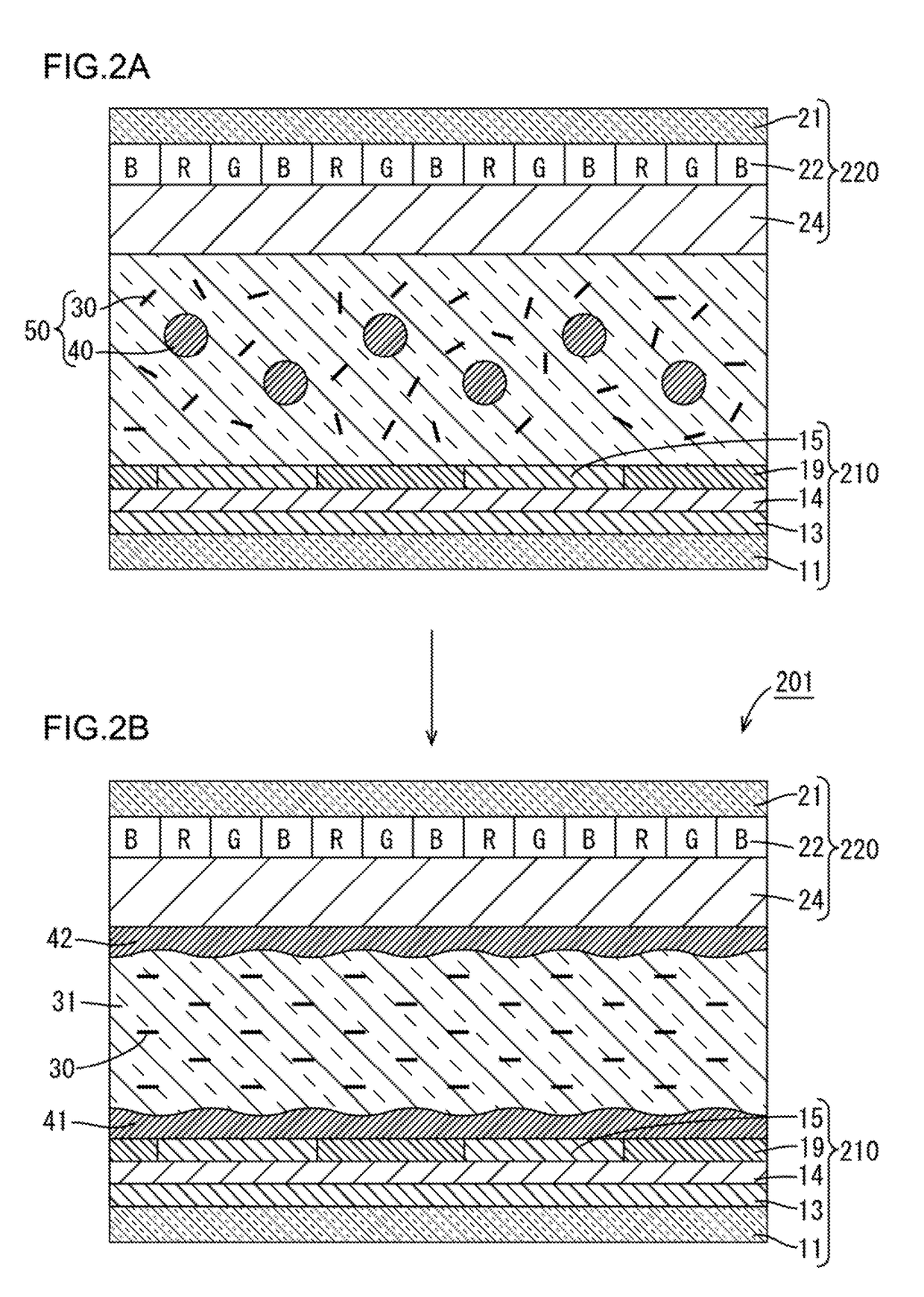
[0080]A second embodiment is explained using FIGS. 2A and 2B. The present second embodiment exemplifies a liquid crystal display including a counter substrate 220 having a color filter layer 22 and an intracellular phase difference layer 24. In the present second embodiment, an array substrate 210 has a conventional alignment film 19, and the counter substrate 220 has no alignment film, unlike the first embodiment. Hereinafter, the same structures as those in the first embodiment are marked with the same numbers, and overlapped explanations are omitted (the same applies to the third embodiment and the fourth embodiment). FIG. 2B shows an IPS mode liquid crystal cell 201 in which a liquid crystal material 30 is horizontally aligned relative to the two substrates 210 and 220 in a liquid crystal layer 31.

[0081](Counte...

third embodiment

isplay Having Alignment Division Control Structure, Including Array Substrate Having NQD-Containing Organic Insulating Film but Having No Alignment Film, and Counter Substrate Having Alignment Film Configured to Control Pre-Tilt Angle of Liquid Crystal Material to Predetermined Range

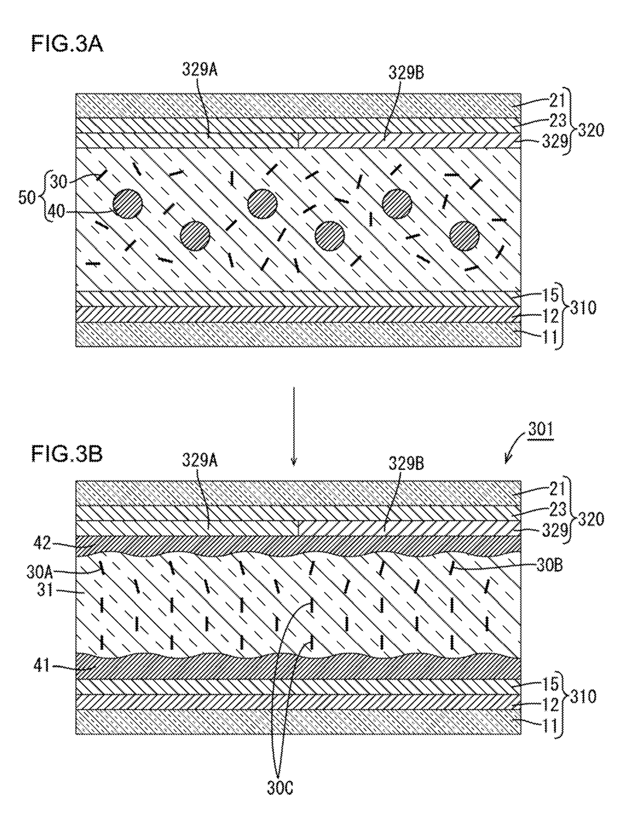
[0096]A third embodiment is explained using FIGS. 3A and 3B. The present third embodiment is different from the first embodiment in that a pre-tilt angle having a predetermined range is imparted to a liquid crystal material on the side of a counter substrate 320 having a conventional alignment film 329, and the display has an alignment division control structure. In addition, in the first embodiment, the structure in which the pixel electrodes 15 and the common electrode 13 are formed in the array substrate 10 has been described, but in the present third embodiment, the common electrode is not formed in the array substrate 310, and a structure in which a counter electrode 23 is formed in the counter subs...


PUM

PropertyMeasurementUnit
Angleaaaaaaaaaa
Angleaaaaaaaaaa
Angleaaaaaaaaaa

Abstract

A liquid crystal display includes a pair of substrates, a liquid crystal layer, and an alignment-controlling layer. The liquid crystal layer is disposed between the pair of substrates and includes a liquid crystal material. The alignment-controlling layer, which is formed by polymerization of a polymerizable monomer added to a liquid crystal composition forming the liquid crystal layer so as to be brought into contact with the liquid crystal layer, and controls an alignment of the liquid crystal material to the substrate at a predetermined angle. One substrate of the pair of substrates has an alignment film coated and formed so as to be brought into contact with the alignment-controlling layer, and the other substrate has no alignment film.

Description

CROSS REFERENCE TO RELATED APPLICATION[0001]This application claims priority from Japanese Patent Application No. 2017-172937 filed on Sep. 8, 2017. The entire contents of the priority application are incorporated herein by reference.TECHNICAL FIELD[0002]The technology disclosed in the present specification relates to a liquid crystal display and a production method therefor.BACKGROUND[0003]A liquid crystal display has a liquid crystal panel on which information such as images is displayed, and the liquid crystal panel has a structure in which, roughly, a liquid crystal layer is sealed between a pair of glass substrates. The pair of substrates includes an array substrate (a pixel electrode substrate, an active matrix substrate, and an element substrate) on which switching elements (such as TFT) and pixel electrodes are provided in an array shape (aligned shape), and a counter substrate disposed opposite thereto. When a voltage is applied to between a common electrode provided on the...

Claims


Application Information

Patent Timeline
IPC IPC(8): G02F1/1337G02F1/1333G02F1/13363
CPCG02F1/133711G02F1/133345G02F1/13363G02F1/133753G02F1/13378G02F2001/133765G02F2202/02G02F2001/133757G02F1/133723G02F2202/023C09K19/56C09K2019/0448G02F1/133565G02F1/133738G02F1/133742G02F1/133757
Inventor MIZUSAKI, MASANOBU
Owner SHARP KK
Why Eureka
Try Eureka