Photoelectric device and substrate thereof
a photoelectric device and substrate technology, applied in the field of photoelectric devices, can solve the problems of low heat dissipation efficiency, uneven thermal distribution, and degrade the reliability of the entire photoelectric device, and achieve the effects of enhancing the heat conducting effect of the die bonding region, improving the structure of the substrate, and reducing temperature differences
- Summary
- Abstract
- Description
- Claims
- Application Information
AI Technical Summary
Benefits of technology
Problems solved by technology
Method used
Image

Examples
first embodiment
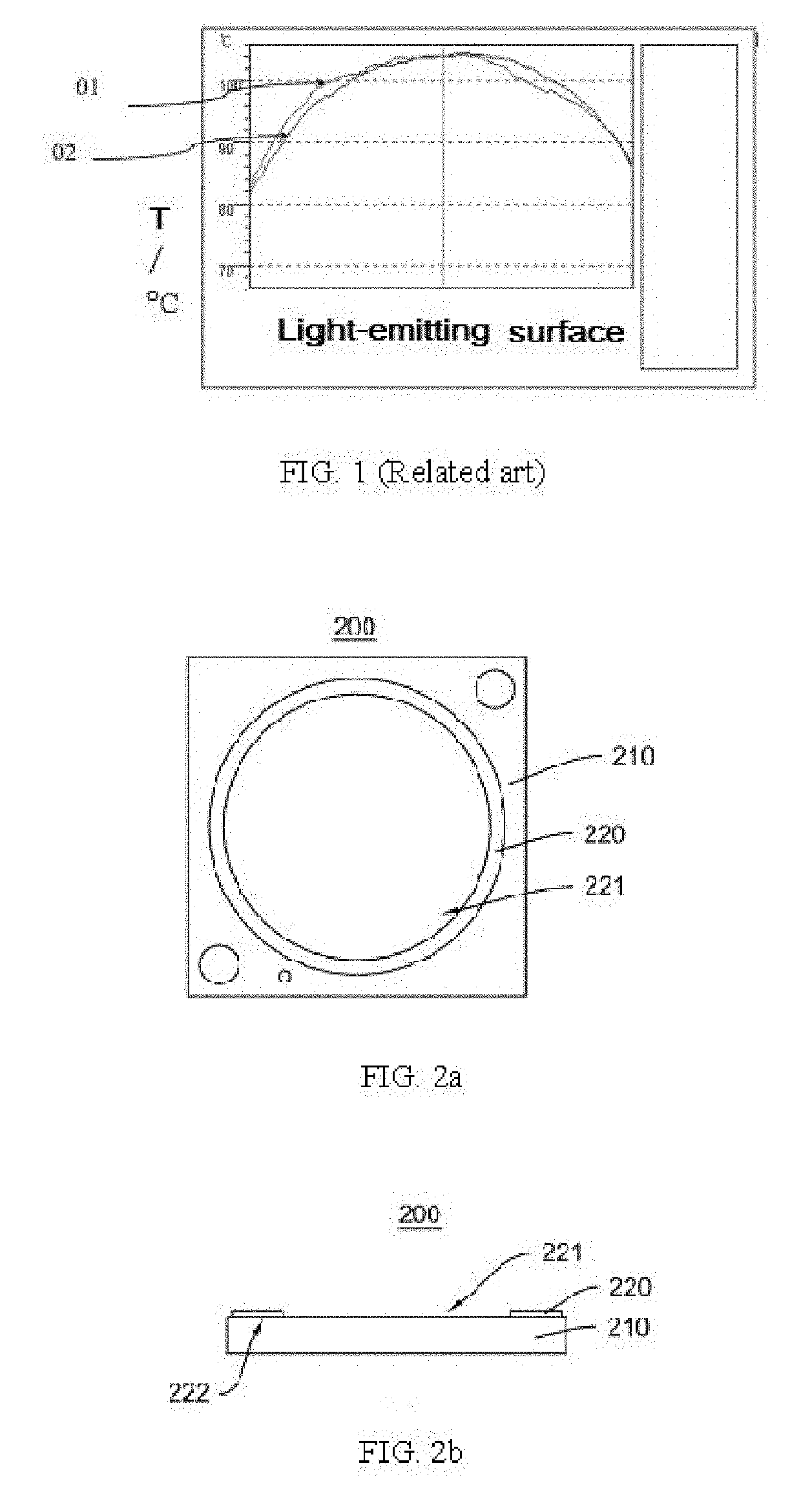
[0035]As shown in FIG. 2a, the embodiment provides a substrate 200, configured for securing of a photoelectric device chip(s) such as a light-emitting diode (LED) chip(s) (not shown). The substrate of the embodiment has an improved heat dissipation structure, especially adapting for centralized securing of large amounts of LED chips with high power density (whose power density is larger than 0.2 W / mm2); the improved heat dissipation structure allows the temperature of the light-emitting surface to be well-distributed, which guarantees the reliability of LED chips.
[0036]As shown in FIG. 2a and FIG. 2b, the substrate 200 of the embodiment includes a metal base 210 and a dielectric layer 220.
[0037]The metal base 210 includes a die bonding region 221 and a peripheral region 222 surrounding the die bonding region 221. The die bonding region 221 is configured for securing of the photoelectric device chips (not shown).
[0038]The dielectric layer 220 is disposed on the metal base 210 and loc...
second embodiment
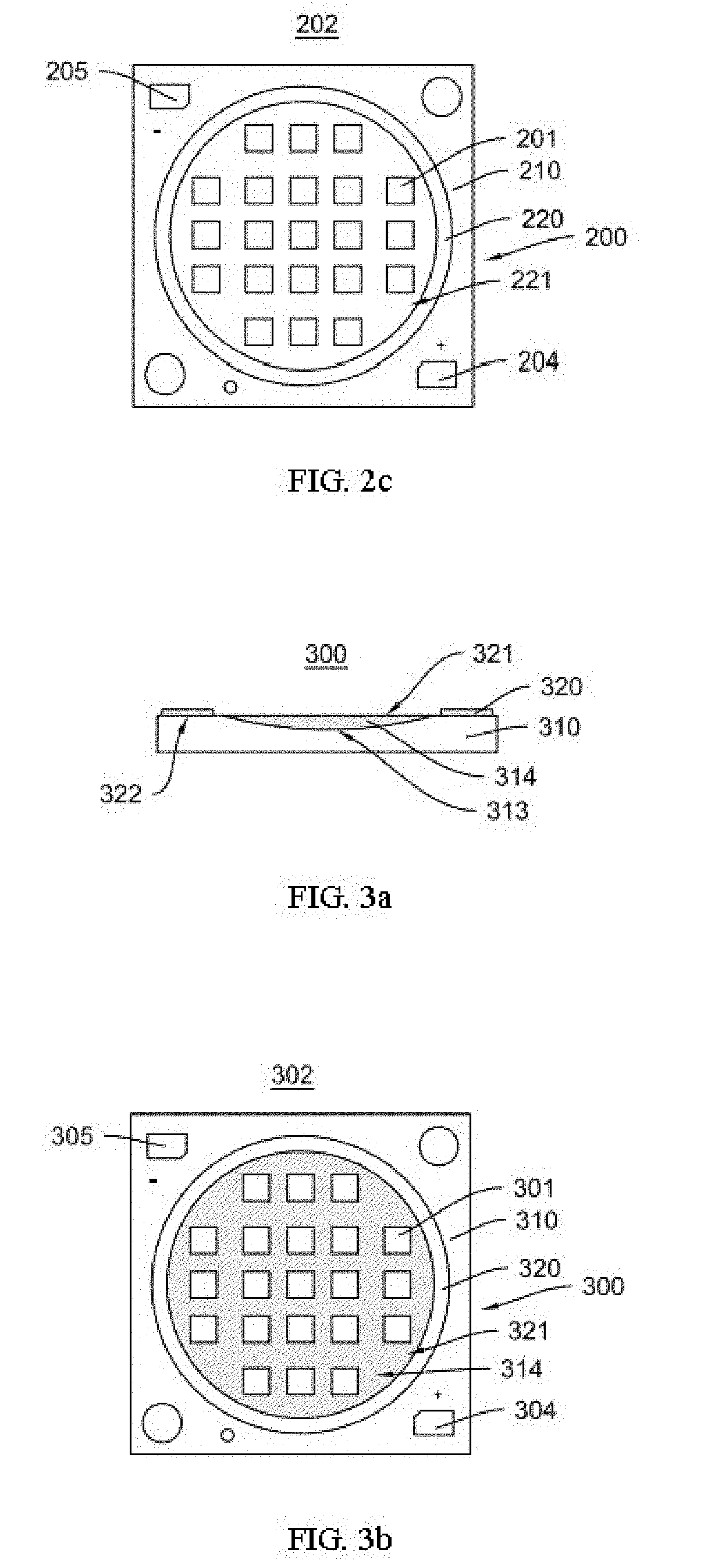
[0049]As shown in FIG. 3a, a substrate 300 of the embodiment is analogous / similar to that of the first embodiment, which is configured for securing of a photoelectric device chip / photoelectric device chips (not shown). The substrate 300 includes a metal base 310 and a dielectric layer 320.
[0050]Similarly to the first embodiment, the metal base 310 includes a die bonding region 321 and a peripheral region 322 surrounding the die bonding region 321. The die bonding region 321 is configured for securing the photoelectric device chip(s) (not shown) thereon.
[0051]The dielectric layer 320 is disposed on the metal base 310 and located in the peripheral region 322 to define the die bonding region 321. In general, a geometrical center of the metal base 310 is corresponding to the center of the die bonding region.
[0052]The material of the metal base 310 can be a mirror aluminum, whose CTE generally is 23˜24 ppm / C. The thickness of the metal base 310 can be various specifications which are in ...
third embodiment
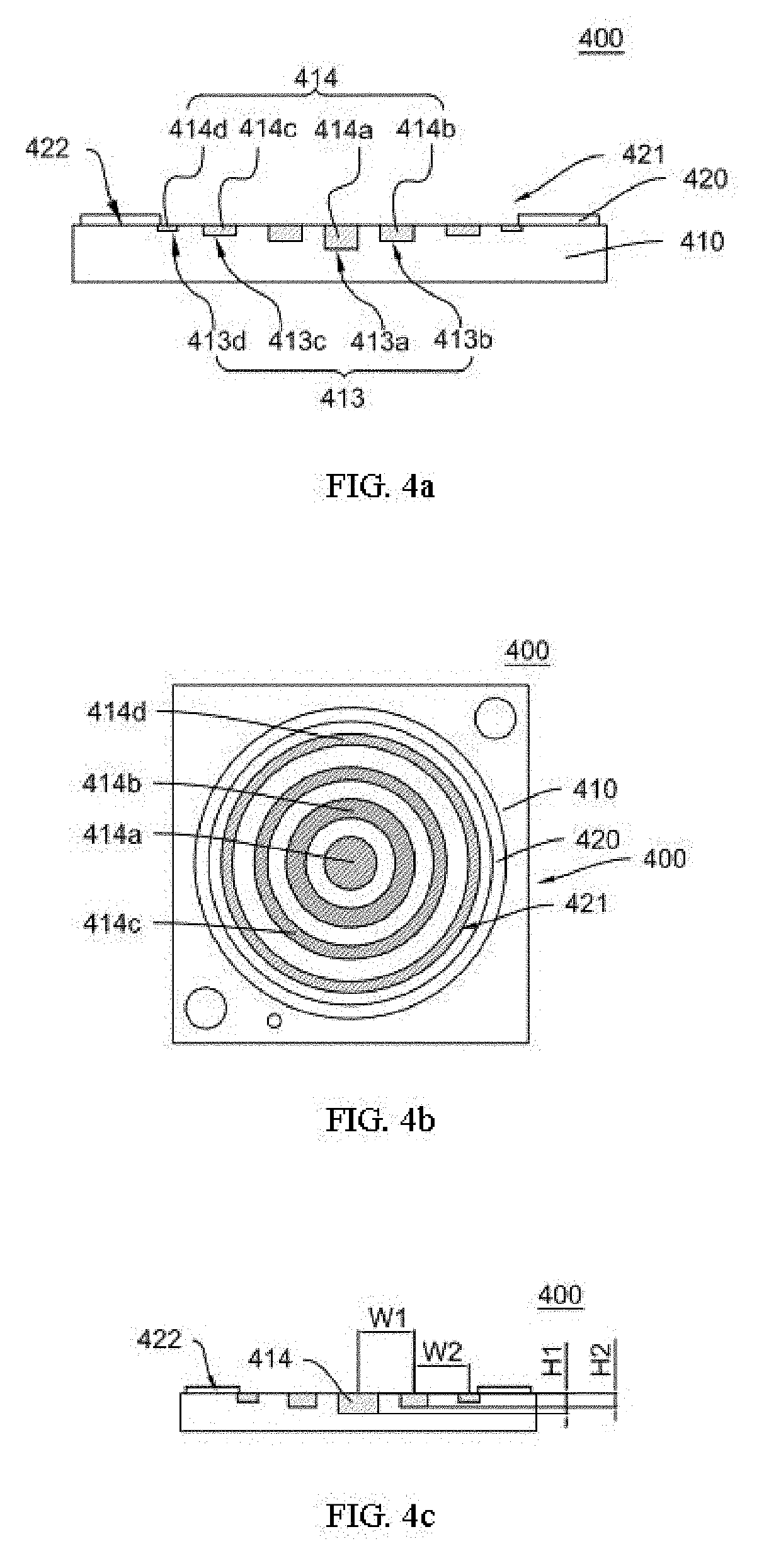
[0060]A substrate 400 of the embodiment is analogous to that of the second embodiment. A difference is that the embodiment further improves the structure of the thermally conductive filler.
[0061]As shown in FIG. 4a and FIG. 4b, a metal base 410 of the embodiment further includes: defining numerous grooves 413 corresponding to the die bonding region 421. For instance, the embodiment includes a first groove 413a, a second groove 413b, a third groove 413c and a fourth groove 413d. The numerous grooves 413 are filled with thermally conductive fillers 414. For example, the embodiment includes a first filler 414a, a second filler 414b, a third filler 414c and a fourth filler 414d to enhance the heat conducting ability for promoting the heat dissipation efficiency of the metal base 410 with the die bonding region 421 and achieving the objective of reducing the temperature of geometrical center of the light-emitting surface 410.
[0062]The CTE of the thermally conductive fillers 414 is prefer...
PUM
| Property | Measurement | Unit |
|---|---|---|
| temperature | aaaaa | aaaaa |
| temperature | aaaaa | aaaaa |
| thickness | aaaaa | aaaaa |
Abstract
Description
Claims
Application Information
 - R&D
- Intellectual Property
- Life Sciences
- Materials
- Tech Scout
- Unparalleled Data Quality
- Higher Quality Content
- 60% Fewer Hallucinations
Browse by: Latest US Patents, China's latest patents, Technical Efficacy Thesaurus, Application Domain, Technology Topic, Popular Technical Reports.
© 2025 PatSnap. All rights reserved.Legal|Privacy policy|Modern Slavery Act Transparency Statement|Sitemap|About US| Contact US: help@patsnap.com