Global shutter pixel circuit and method for computer vision applications

a technology of shutter pixel and computer vision, applied in the field of image sensor pixel circuits, can solve the problems of large size, high power consumption, drawbacks of conventional cmos pixel sensors, etc., and achieve the effects of low capacitance, fast time-of-flight gating, and fast signal transfer

Active Publication Date: 2019-06-13
MAGIC LEAP
View PDF0 Cites 30 Cited by
  • Summary
  • Abstract
  • Description
  • Claims
  • Application Information

AI Technical Summary

Benefits of technology

[0010]In embodiments of the present invention, a ToF depth measurement can be carried out by illuminating the object or scene with light pulses using a sequence of temporal windows and applying a convolution process to the optical signal received at the sensor. Embodiments of the invention provide an improved pixel circuit and a method that has fast time-of-flight gating using a single control line per pixel. The pixel circuit can be implemented based on an improved global shutter CMOS image sensor process flow. In some embodiments, a shuttering mechanism based on static gate integration combined with dynamic LDM (lateral draining modulation) can be realized using either a global reset gate or drain voltage modulation. Fast signal transfer is enabled in the pixel circuit using low capacitance and low resistance device structure and interconnect lines.

Problems solved by technology

However, conventional CMOS pixel sensors tend to have drawbacks such as large size and high power consumption.

Method used


Image

  • Global shutter pixel circuit and method for computer vision applications
  • Global shutter pixel circuit and method for computer vision applications
  • Global shutter pixel circuit and method for computer vision applications

Examples


Embodiment Construction

[0081]Embodiments of the present invention provide a system and method that enable ToF depth measurement with calibration to provide high accuracy using optical feedback and fast image processing. A range of depth measurements can be calibrated for each frame with minimal effect on sensor performance and power consumption.

[0082]The description below is presented with reference to a series of drawing figures enumerated above. These diagrams are merely examples, and should not unduly limit the scope of the claims herein. In connection with the various aspects illustrated and described, one of ordinary skill in the art would recognize other variations, modifications, and alternatives.

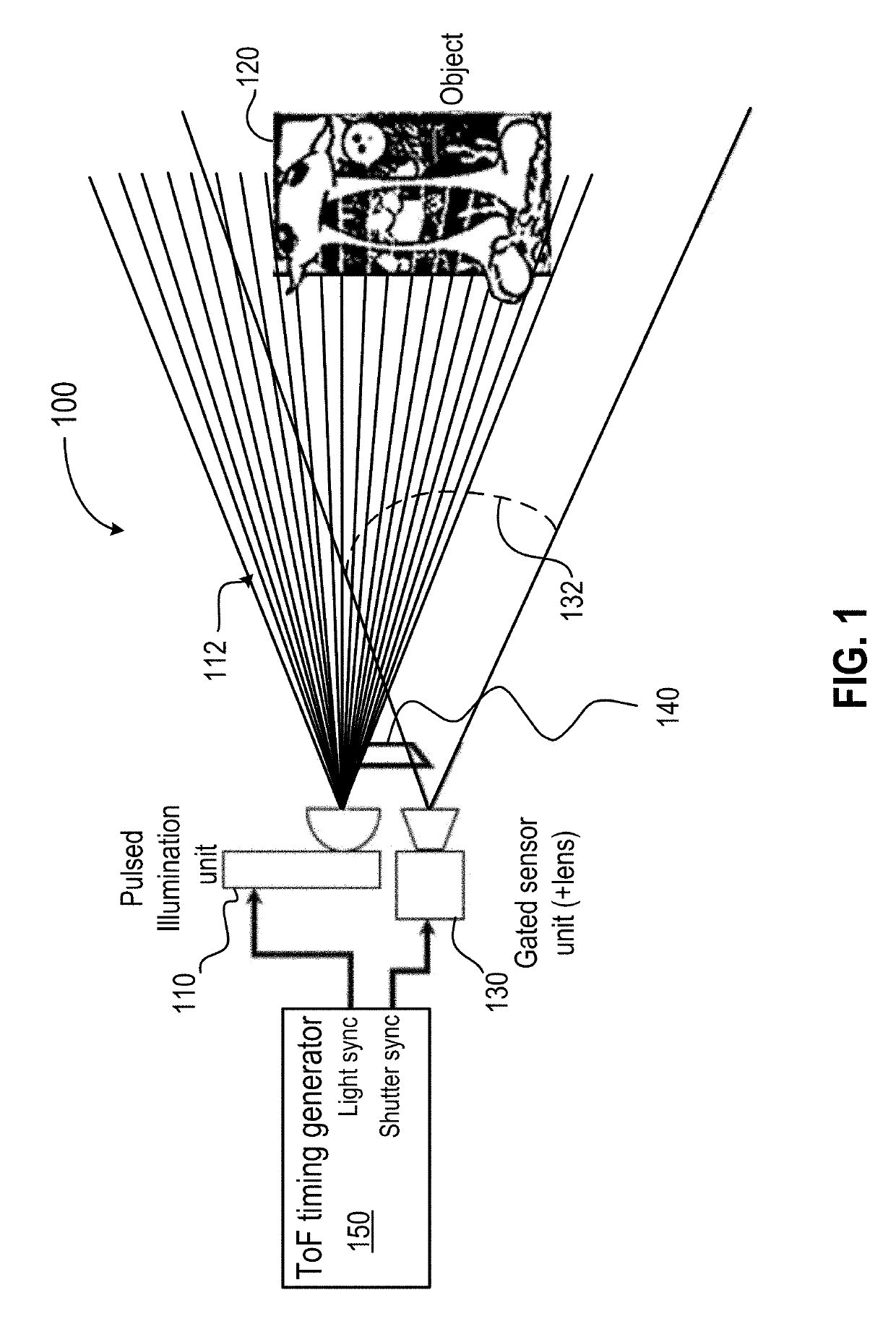
[0083]FIG. 1 is a diagram illustrating a time-of-flight (ToF) imaging system for depth measurement according to an embodiment of the present invention. As shown in FIG. 1, a time-of-flight (ToF) imaging system 100, also referred to as a ToF digital camera, includes an illuminator 110 to transmit light puls...


PUM


Abstract

An image sensor device includes a plurality of pixel cells arranged in a pixel array, a control circuit for controlling an exposure phase and a sampling phase of the image sensor device. Each of the plurality of pixel cells includes a photodiode, a storage diode, and a floating diffusion region. The control circuit is configured to activate the photodiode in a plurality of time windows to sense light reflected from a target as a result of a corresponding plurality of emitted light pulses, with a pre-determined delay time between each time window and a corresponding emitted light pulse. The photodiode can be activated using a plurality of bias voltage pulses or a plurality of global shutter signal pulses.

Description

CROSS-REFERENCES TO RELATED APPLICATIONS[0001]This application claims the benefit of U.S. Provisional Patent Application No. 62 / 598,390, filed on Dec. 13, 2017, the contents of which are hereby incorporated by reference in their entirety.[0002]The following regular U.S. patent applications (including this one) are being filed concurrently, and the entire disclosure of the other applications are incorporated by reference into this application for all purposes:[0003]U.S. patent application Ser. No. 16 / ______, filed on Dec. 13, 2018, entitled “GLOBAL SHUTTER PIXEL CIRCUIT AND METHOD FOR COMPUTER VISION APPLICATIONS;” AND[0004]U.S. patent application Ser. No. 16 / ______, filed on Dec. 13, 2018, entitled “DIFFERENTIAL PIXEL CIRCUIT AND METHOD OF COMPUTER VISION APPLICATIONS.”FIELD OF THE INVENTION[0005]Embodiments of the present invention relate generally to image sensor pixel circuits and methods for time-of-flight (ToF) depth measurement systems.BACKGROUND OF THE INVENTION[0006]Image se...

Claims


Application Information

Patent Timeline
Patent Type & Authority Applications(United States)
IPC IPC(8): H01L27/146H04N5/341
CPCH01L27/14609H04N5/341H01L27/14643H01L27/1463H01L27/14641H01L27/14605G01S7/4814G01S7/4816G01S7/4863G01S7/4865G01S17/894H04N23/60H04N25/77G01S11/00H04N23/73H04N25/40H04N25/778H04N25/771G01S17/08H04N25/705
Inventor TADMOR, EREZCOHENYAHAN, GIORA
Owner MAGIC LEAP
Why Eureka
Try Eureka