Waveguide interface and printed circuit board launch transducer assembly and methods of use thereof

a technology of waveguide interface and printed circuit board, which is applied in the direction of waveguide, printed circuit non-printed electric components association, high frequency circuit adaptation, etc., can solve the problems of increasing the cost of wire bonding, and prone to errors and yield problems, so as to eliminate the need for expensive wire bonding

Active Publication Date: 2019-07-04
VUBIQ
View PDF1 Cites 2 Cited by
  • Summary
  • Abstract
  • Description
  • Claims
  • Application Information

AI Technical Summary

Benefits of technology

[0009]This exemplary technology provides a number of advantages including providing a printed circuit board assembly including an integrated launch transducer device that is compatible with wafer level chip scale packaging techniques for millimeter wave semiconductor integrated circuits. The printed circuit board assembly with the integrated transducer device m...

Problems solved by technology

The stub or paddle launch is orthogonal to the waveguide cavity, also requiring a split-cavity type of assembly method, creating additional expense.
Wire bonding is an expensive process and is prone to errors and yield problems.
However, standard launch transduce...

Method used


Image

  • Waveguide interface and printed circuit board launch transducer assembly and methods of use thereof
  • Waveguide interface and printed circuit board launch transducer assembly and methods of use thereof
  • Waveguide interface and printed circuit board launch transducer assembly and methods of use thereof

Examples


Embodiment Construction

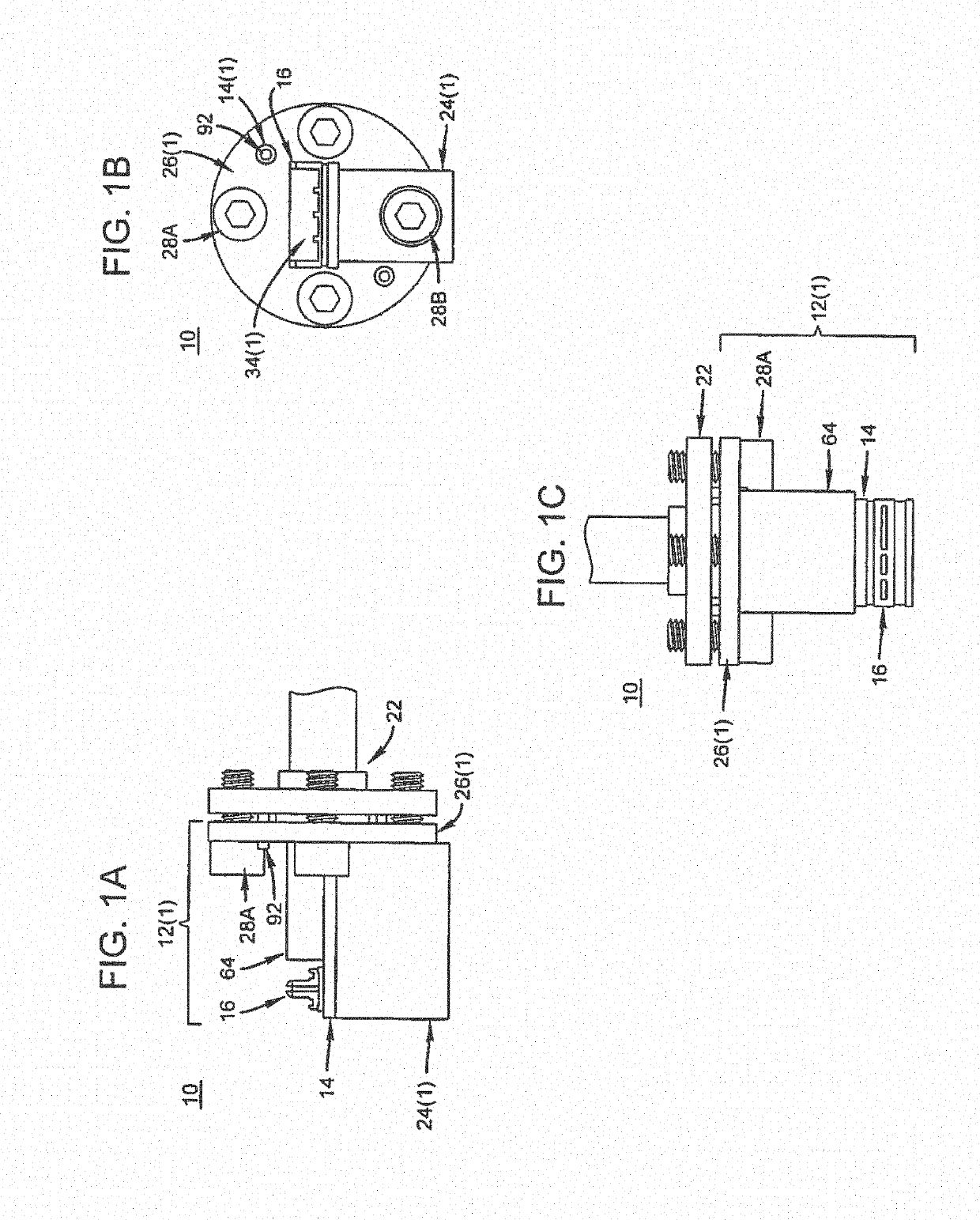
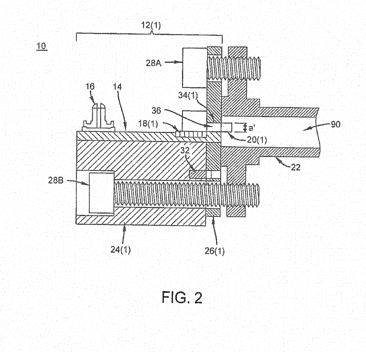
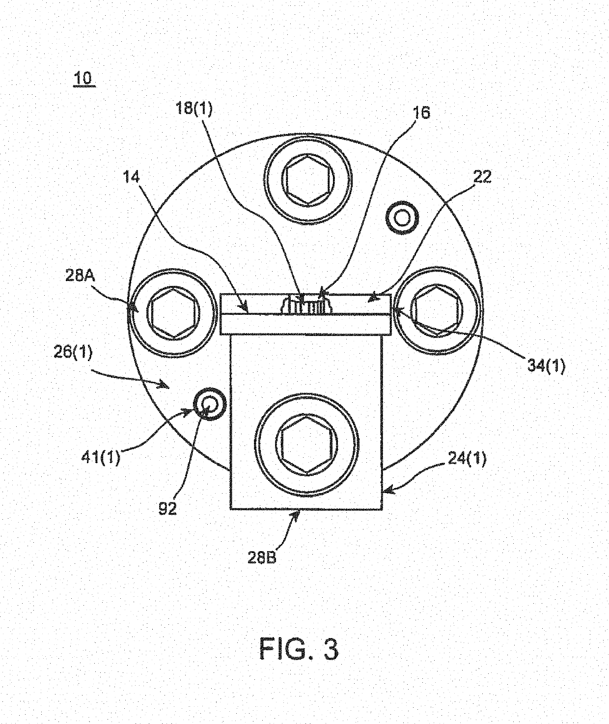
[0046]Referring to FIGS. 1A-4, an example of a waveguide assembly 10 includes an exemplary waveguide interface 12(1), a printed circuit board assembly 14 including a connector 16, a communication device 18(1), and a launch transducer 20(1), and a waveguide flange 22, is illustrated, although the waveguide assembly 10 could include other types and numbers of assemblies, devices, components, and / or other elements in other configurations. In another example, as described below with respect to FIGS. 20-24C, the waveguide assembly 10 may incorporate a printed circuit board assembly 140(1) or 140(2) formed from a plurality of layers with an integrated launch transducer formed from one of the layers.

[0047]As described below, the waveguide assembly 10 may be utilized for electromagnetic transmission and electromagnetic reception. Both the transmission context and the reception context equally apply due to the Lorentz electromagnetic reciprocity theorem. This exemplary technology provides a ...


PUM


Abstract

A printed circuit board assembly comprising a plurality of layers. At least one of the plurality of layers is formed of a dielectric material and has an extended portion extending beyond the other layers in the plurality of layers. A first metallic layer is located on at least a portion of the extended portion of the dielectric layer. The first metallic layer and the dielectric layer are configured to form a launch transducer comprising one or more transmission lines and a transducer element coupled to the one or more transmission lines. The transducer element is configured to propagate millimeter wave frequency signals.

Description

FIELD[0001]The present disclosure relates generally to a waveguide interface and printed circuit board launch transducer assembly for microwave and millimeter wave radio frequency technologies. More specifically, the present disclosure relates to a waveguide interface including a printed circuit board with an integrated launch transducer that may utilized with surface mounted millimeter wave semiconductor integrated circuits.BACKGROUND[0002]As the semiconductor industry continues to increase circuit complexity and density by reduction of process node geometries, operating signal frequencies continue to increase. It is now possible to obtain semiconductors that operate well into the millimeter wave region of radio spectrum (30 GHz to 300 GHz). Traditionally, the types of semiconductors used have been in the category of “III-V” types, indicating that the semiconductor compounds have been derived from periodic table elements in the third and fifth columns, such as gallium arsenide (GaA...

Claims


Application Information

Patent Timeline
IPC IPC(8): H01P3/12H01P5/10H01P1/04H05K1/02
CPCH01P3/121H01P5/10H01P1/042H05K1/0298H05K1/0296H05K3/0044H05K1/18H01P3/082H05K2203/02H01P5/107H05K1/0237H01L2224/49433H01L2224/49175H01L2224/05554
Inventor PETTUS, MICHAEL GREGORYEISENHART, ROBERT LEE
Owner VUBIQ
Why Eureka
Try Eureka