Method and system for correction of optical proximity effect

US20190212643A1Active Publication Date: 2019-07-11CSMC TECH FAB2 CO LTD
1 Cites 1 Cited by

Patent Information

Authority / Receiving Office
US · United States
Current Assignee / Owner
Publication Date
2019-07-11

Smart Images

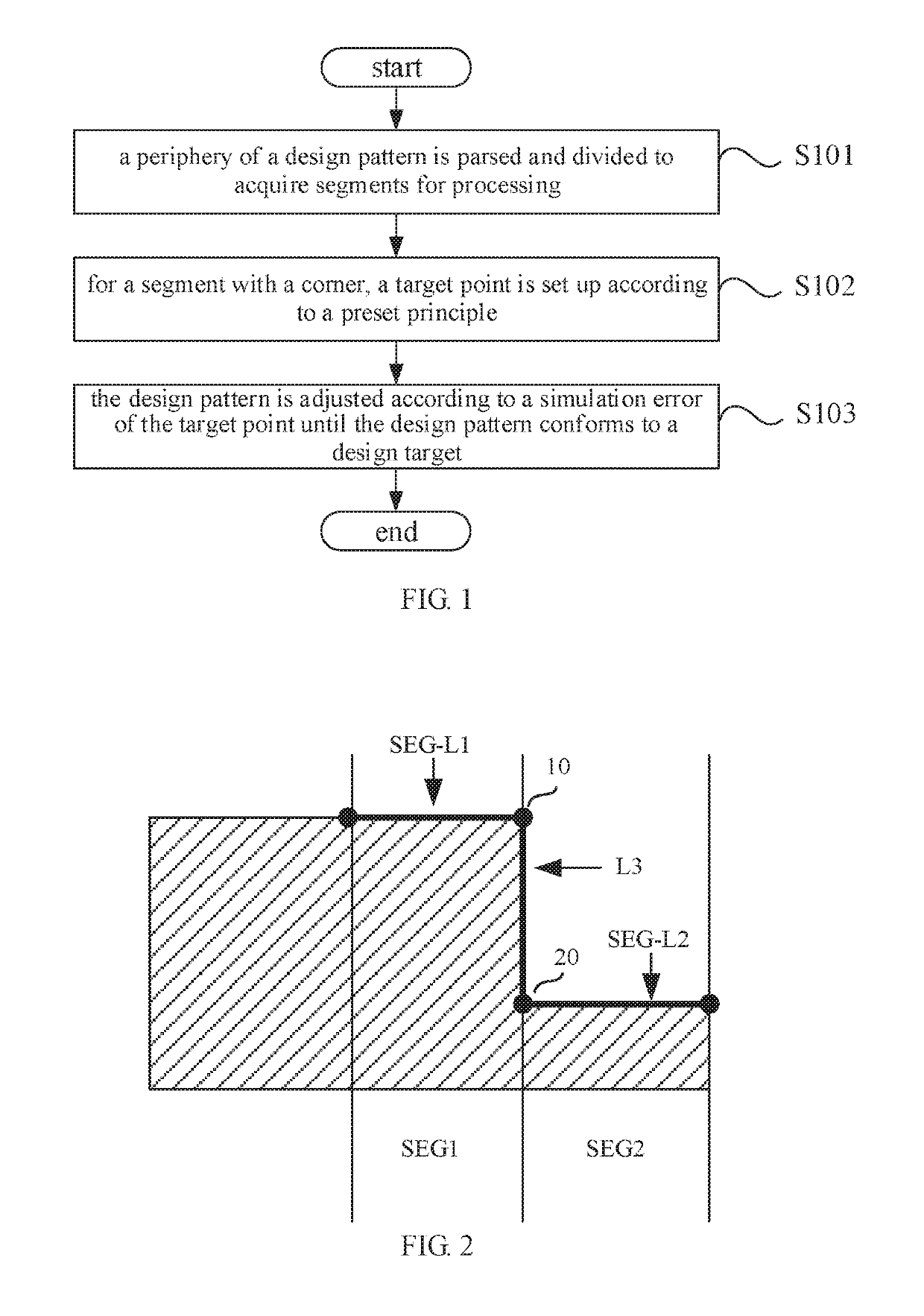
  • Figure 1
    Figure 1
  • Figure 2
    Figure 2
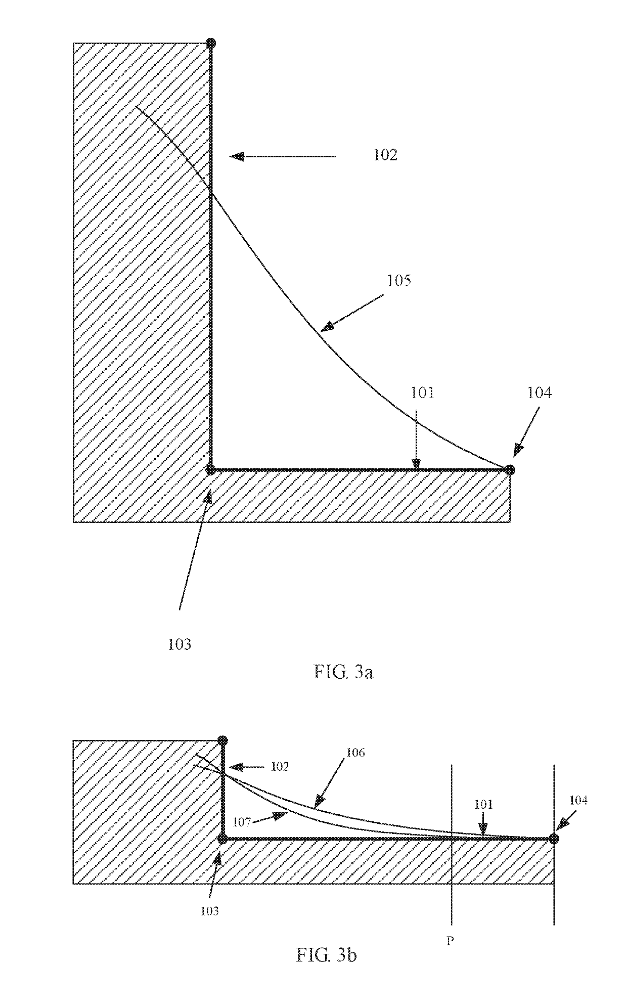
  • Figure 3
    Figure 3
Patent Text Reader

Abstract

A method for correction of an optical proximity effect, comprising: parsing and dividing the periphery of a design pattern to obtain segments to process; for a segment having a corner comprising a segment side (101) and an adjacent side (102) forming a corner relation with the segment side, setting a target point according to the following principle: when the length of the adjacent side (102) is greater than a preset length, the target point is set at the location of the outer end point (104) of the segment side; when the length of the adjacent side (102) is less than or equal to the preset length, the target point is set between the vertex (103) of the corner and the outer end point (104) of the segment side, and the less the length of the adjacent side (102), the further the target point from the location of the outer end point (104); and adjusting, according to a simulation difference of the target point, the design pattern until it conforms to a design target.
Need to check novelty before this filing date? Find Prior Art

Description

FIELD OF THE INVENTION

[0001] The present disclosure relates to a field of semiconductor technology, and particularly relates to a method and system for correction of optical proximity effect (OPE).BACKGROUND OF THE INVENTION

[0002] With the development of semiconductor technology, the critical dimension of the key levels in the semiconductor process, such as the active region level, the gate-oxide level, or the metal wiring level, is increasingly smaller, which is approximating or even less than the wave length of the optical wave used in the photolithography technique. As such, in the photolithographic process, due to the diffraction and interference of light, certain distortion and deviation exist between the mask pattern and the photo pattern obtained on the silicon wafer actually.

[0003] Such an error in the photolithography directly affect the performance and the yield of circuits. In order to eliminate such error as much as possible, an effective way is to adopt OPE correction. A s...

Examples

Embodiment Construction

[0021]The present disclosure will be described in the following with reference to the accompanying drawings and the embodiments in order to make the above objects, features and advantages of the present disclosure more apparent.

[0022]The specific embodiments will be described in detail in combination with the accompanying drawings.

[0023]The method in the following embodiments is related to a method of how to place a target point in the OPE correction. There are a lot of steps included in the OPE correction method, and the placement of target point is one of the aspects. The embodiments below will not describe all the steps, only contents relevant to the placement of the target point are described.

[0024]FIG. 1 is a flowchart of a method for correction of OPE according to an embodiment, the method includes the following steps of:

[0025]In step S101, an outer edge of a design pattern is parsed and divided to obtain segments to be processed. As the design pattern is usually complicated, ...