Optoelectronic device based on a surface-trapped optical mode

a surface-trapped optical mode and optoelectronic technology, applied in the direction of laser optical resonator construction, laser details, semiconductor lasers, etc., can solve the problems of difficult to focus to a single spot of light coming out of the device, adversely affecting multiple applications like optical data transmission, and inability to efficiently couple to a single mode fiber

Active Publication Date: 2019-07-18
VI SYST GMBH
View PDF0 Cites 3 Cited by
  • Summary
  • Abstract
  • Description
  • Claims
  • Application Information

AI Technical Summary

Benefits of technology

[0021]An optoelectronic device employs a surface-trapped TM-polarized optical mode existing at a boundary between a distributed Bragg reflector and a homogeneous medium, dielectric or air. The device contains a resonant optical cavity surrounded by two DBRs, and an additional DBR section on top supporting the surface-trapped mode. Selective chemical transformation, like selective oxidation, etching or alloy composition intermixing form a central core and a periphery having different vertical profiles of the refractive index. Therefore, the longitudinal VCSEL mode in the core is non-orthogonal to the surface-trapped mode in the periphery, and the two modes can be transformed into each other. Such transformation allows fabrication of a number of optoelectronic devices and systems like a single transverse mode VCSEL, an integrated optical circuit operating as an optical amplifier, an integrated optical circuit combining a VCSEL and a resonant cavity photodetector, etc.

Problems solved by technology

These phenomena make focusing to a single spot of the light coming out of the device hardly possible and adversely affects multiple applications like optical data transmission.
Thus, it makes efficient coupling to a single mode fiber questionable.
Similar problems occur also in tilted cavity laser, tilted wave laser, passive cavity laser, near-field laser.
However, as each laser emits independently, the resulting beam is not focusable to a small spot also in this case.
However, the need in a complex optical system makes the device bulky and expensive.
This could give a possibility of a leakage of the VCSEL optical mode from the non-oxidized core region to the oxidized periphery region.
However, the leakage of the VCSEL optical mode to the oxidized periphery occurs via the doped semiconductor layers, typically, via p-doped semiconductor layers.
Once the leakage component of the optical field is not considered as a lost field but as a means of coupling of VCSELs in a coherent array, the losses due to the free carrier absorption is not desirable.

Method used


Image

  • Optoelectronic device based on a surface-trapped optical mode
  • Optoelectronic device based on a surface-trapped optical mode
  • Optoelectronic device based on a surface-trapped optical mode

Examples


Embodiment Construction

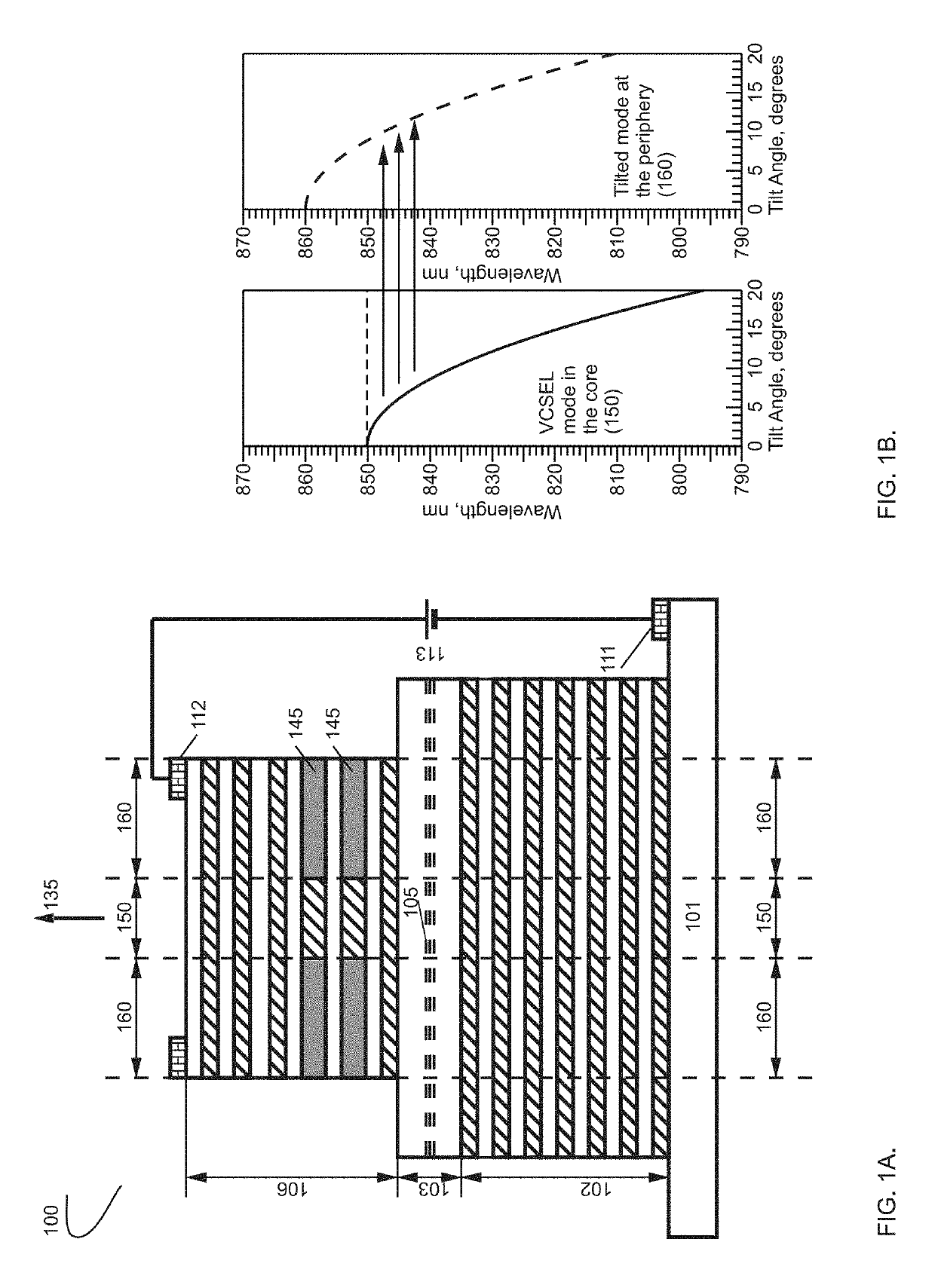
[0047]The present patent application employs the properties of a surface optical wave which can be formed at a boundary between a distributed Bragg reflector (DBR) and the air or at a boundary between a DBR and a thick dielectric layer. Such wave was disclosed in the recent publication by V. A. Shchukin, N. N. Ledentsov, V. P. Kalosha, N. Ledentsov Jr., M. Agustin, J.-R. Kropp, M. V. Maximov, F. I. Zubov, Yu. M. Shernyakov, A. S. Payusov, N. Yu. Gordeev, M. M. Kulagina, A. E. Zhukov, and A. Yu. Egorov, “Virtual cavity in distributed Bragg reflectors”, Optics Express, volume 26, issue 19, of Sep. 17, 2018, wherein this publication is hereby incorporated herein by reference, referred below to as Shchukin'18.

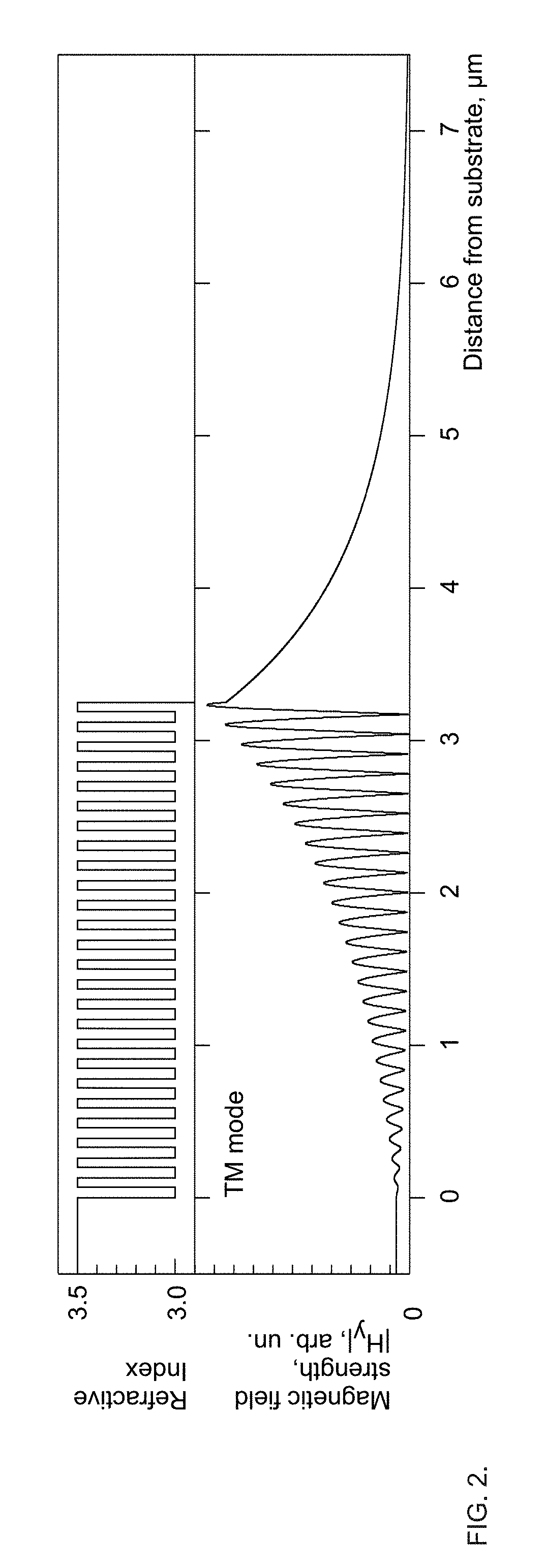
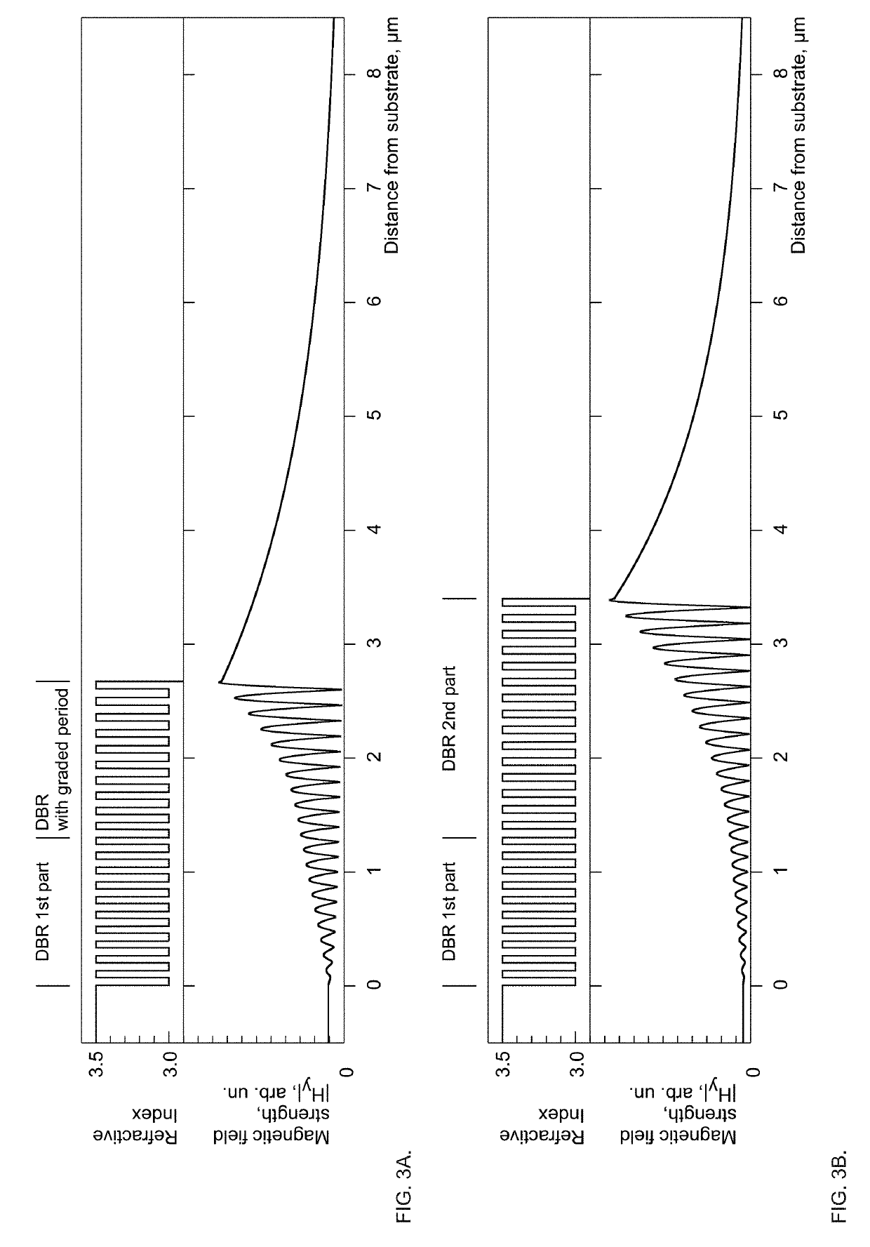
[0048]FIG. 2 illustrates a DBR formed of 25 periods of layers with alternating refractive indices n1=3.5 and n2=3.0, which are typical for Ga(1−x)Al(x)As alloy with a low and a high Al composition, respectively. The thicknesses of the layers equal d1=λ0 / (4n1) and d2=λ0 / (4n2), respe...


PUM


Abstract

An optoelectronic device employs a surface-trapped TM-polarized optical mode existing at a boundary between a distributed Bragg reflector (DBR) and a homogeneous medium, dielectric or air. The device contains a resonant optical cavity surrounded by two DBRs, and an additional DBR section on top supporting the surface-trapped mode. Selective chemical transformation, like selective oxidation, etching or alloy composition intermixing form a central core and a periphery having different vertical profiles of the refractive index. Therefore, the longitudinal VCSEL mode in the core is non-orthogonal to the surface-trapped mode in the periphery, and the two modes can be transformed into each other. Such transformation allows fabrication of a number of optoelectronic devices and systems like a single transverse mode VCSEL, an integrated optical circuit operating as an optical amplifier, an integrated optical circuit combining a VCSEL and a resonant cavity photodetector, etc.

Description

REFERENCE TO RELATED APPLICATIONS[0001]This is a continuation-in-part of U.S. patent application Ser. No. 13 / 771,875, filed Feb. 20, 2013, entitled: “Optoelectronic Device with Resonant Suppression of High Order Optical Modes and Method of Making Same”, and of U.S. patent application Ser. No. 15 / 040,965, filed Feb. 10, 2016, entitled “Optoelectronic Device with Enhanced Lateral Leakage of High Order Transverse Optical Modes into Alloy-Intermixing Regions and Method of Making Same”. The aforementioned applications are hereby incorporated herein by reference.BACKGROUND OF THE INVENTIONField of the Invention[0002]The invention pertains to the field of optoelectronic devices. More particularly, the invention pertains to light emitting devices.Description of Related Art[0003]Light-emitting devices are presently broadly used in multiple applications, particularly in lighting, projection displays, sensing, material processing, optical storage, optical data transmission and in other applica...

Claims


Application Information

Patent Timeline
Patent Type & Authority Applications(United States)
IPC IPC(8): H01S5/183H01S5/10H01S5/02H01S5/22H01S5/20
CPCH01S5/18302H01S5/1021H01S5/1833H01S5/18311H01S5/18352H01S5/0215H01S5/18333H01S5/222H01S5/205H01S5/423H01S2301/166H01S5/18313H01S5/18361H01S5/18377H01S5/18369H01S5/026H01S2301/176H01S5/1035
Inventor LEDENTSOV, NIKOLAYSHCHUKIN, VITALY
Owner VI SYST GMBH
Why Eureka
Try Eureka