Silicon-photonics-based optical switch with low polarization sensitivity
- Summary
- Abstract
- Description
- Claims
- Application Information
AI Technical Summary
Benefits of technology
Problems solved by technology
Method used
Image
Examples
Embodiment Construction
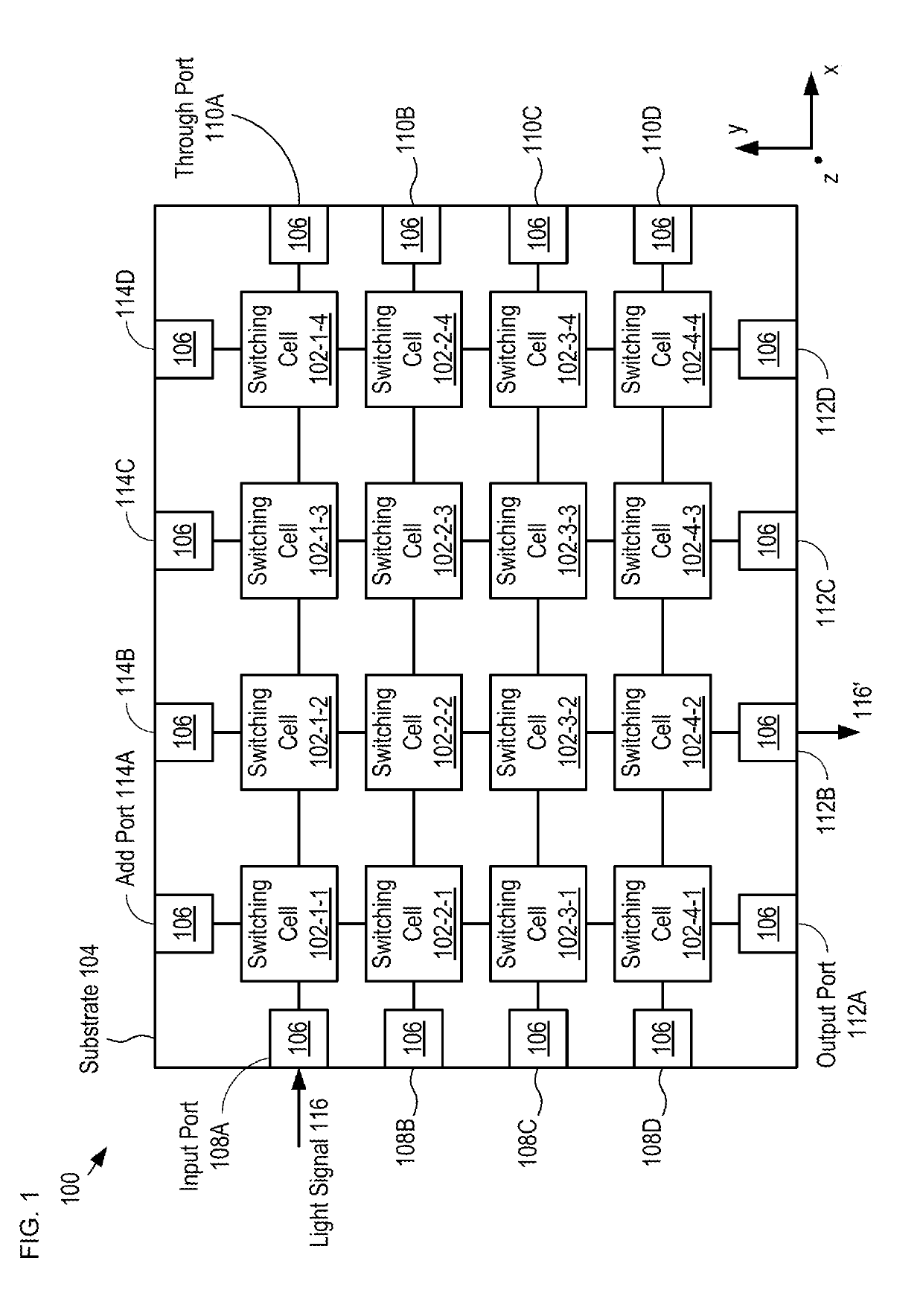
[0046]FIG. 1 depicts a schematic drawing of an optical switching system in accordance with an illustrative embodiment of the present invention. System 100 is an optical cross-connect that includes a 4×4 array of switching-cells 102-1-1 through 102-4-4, each of which is disposed on substrate 104. It should be noted that, although the depicted example comprises three rows and four columns of switching cells, any practical number of rows and / or columns of switching cells can be included in system 100 without departing from the scope of the present invention.
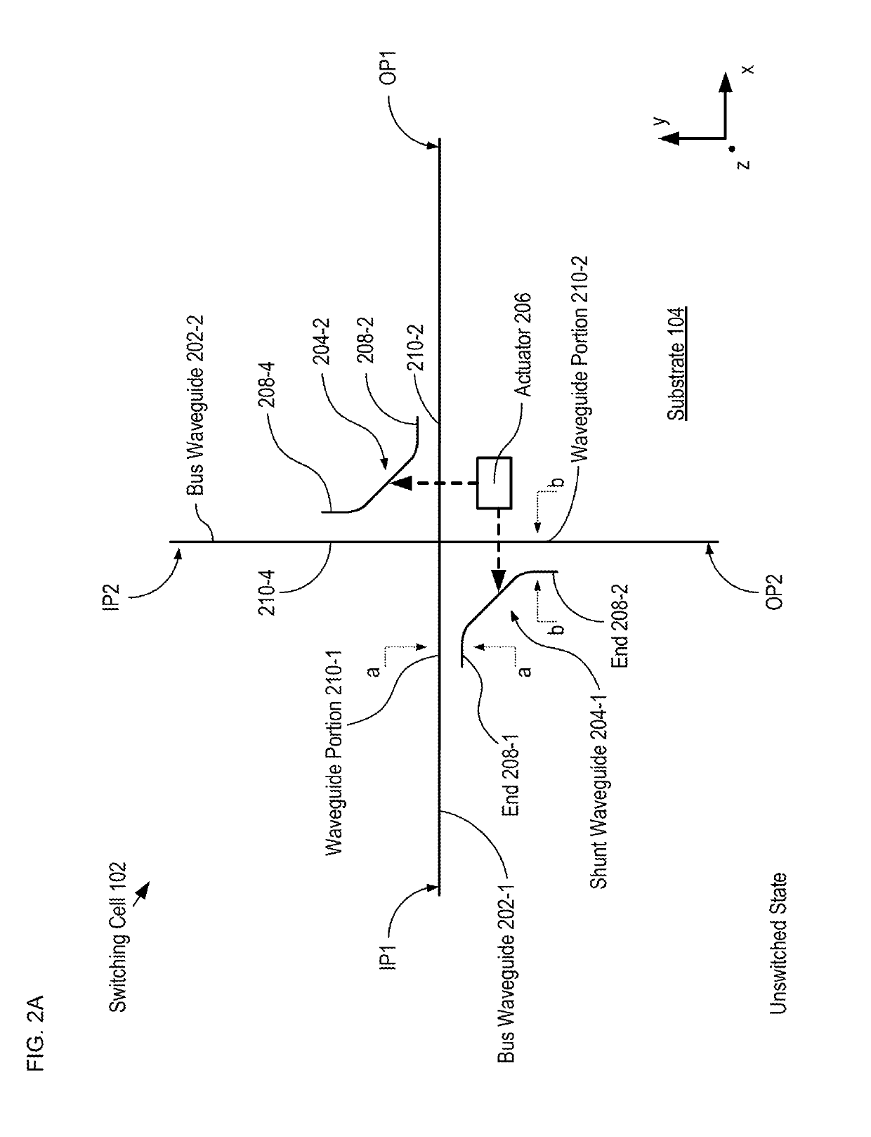
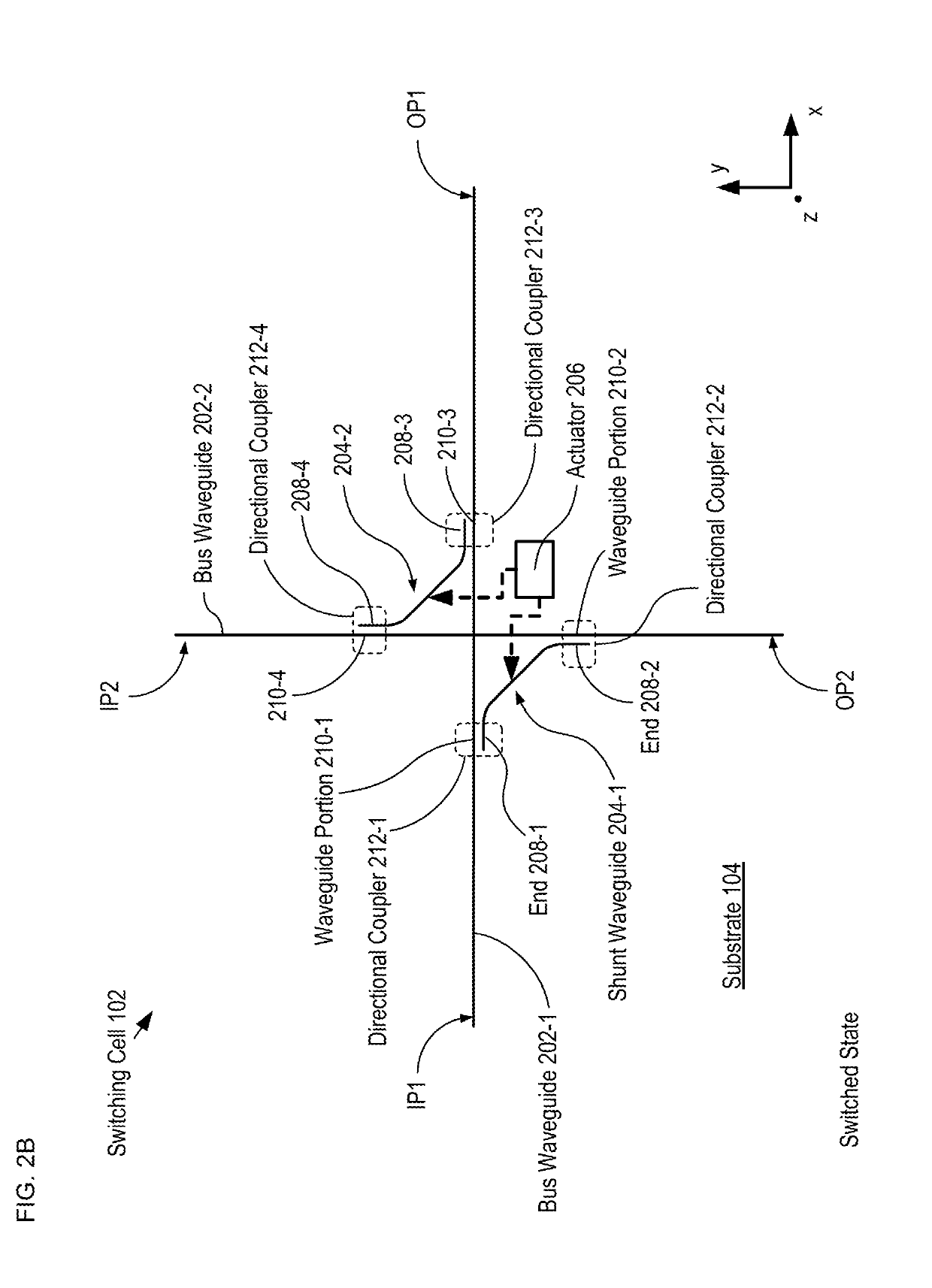
[0047]Each of switching cells 102-1-1 through 102-4-4 (referred to, collectively, as cells 102) is a 2×2 crossbar switch that includes a pair of sub-micron-width bus waveguides and a pair of movable shunt waveguides, whose positions determine the connectivity of the inputs and outputs of the switching cell.
[0048]It is an aspect of the present invention that the silicon-photonic waveguides used in the switching cells of its different...
PUM
 Abstract
Description
Claims
Application Information


