Currently, the size of high-end
semiconductor element packages is becoming larger and larger.
As such, the conductive through holes have a large
pitch therebetween, thus adversely affecting fine-
pitch and fine-line wiring in the core layer.
However, the coreless substrate is thin, has poor rigidity and cannot
resist warping.
Therefore, the coreless substrate is not applicable to the large-size electronic
package 1.
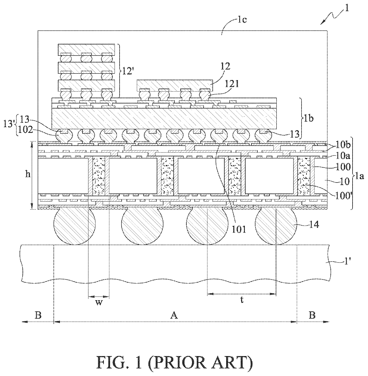
However, the conventional flip-
chip packaging substrate 1a having the core layer 10 applied to packages with high integration and large panel size has some drawbacks.
For example, since the core layer 10 is made of a base material composed of
glass fiber combined with
epoxy resin, due to different CTEs (coefficients of
thermal expansion) between various layers of the flip-
chip packaging substrate 1a and the TSI 1b, the
semiconductor chip 12, the
chipset 12′ and the encapsulant 1c (encapsulating the TSI 1b, the
semiconductor chip 12 and the
chipset 12′), warping may occur during the packaging process and thus lead to a poor bonding between the packaging substrate 1a and the TSI 1b, or a poor connection may occur between the packaging substrate 1a and the circuit board 1′ during the
soldering process.
Further, when the conventional substrate having the core layer is used as a flip-chip packaging substrate 1a with a large panel size, its rigidity and support stresses are insufficient, thus resulting in poor flatness.
Therefore, when it is mounted on the circuit board 1′, stresses may adversely affect the stability of product quality and reliability.
First, the pitch between the conductive through holes 100 cannot be reduced. For instance, due to the
increased thickness of the core layer 10, the size of end surfaces of the conductive through holes 100 will be increased. For example, if the thickness h is 0.8 mm, the
diameter w of the through holes and the pitch between the through holes are typically 150 μm and 300 μm (or more), respectively. If the thickness h is 1.2 mm, the
diameter w will be increased to 200 μm or more (that is, the
diameter w becomes larger), resulting in a larger pitch between the conductive through holes 100. Therefore, the number of the conductive through holes 100 per unit area is reduced, which adversely affects the fabrication of high-density and fine-pitch wiring. As such, in order to meet the demand for more contacts (I / O), the size of the flip-chip packaging substrate 1a must be increased, thus making it more difficult to control warping and greatly increasing the cost.
Second, the
processing cost and difficulty of the conductive through holes 100 increase with the thickness of the core layer 10. For instance, the
increased thickness of the core layer 10 results in deeper conductive through holes 100, thereby increasing the difficulty in performing
electroplating and smoothly filling the filling material 100′ in the deeper conductive through holes 100 and also increasing the
processing cost.
On the other hand, as the conventional large-size electronic
package 1 is developed toward high number of stack layers and
high density, the fabrication processes of the flip-chip packaging substrate 1a and the circuit board 1′ become more and more complicated, and the higher the requirement of precision, the more difficult it is to process the circuit board 1′.
Therefore, the fabrication process of the circuit board 1′ in a large-size
package will face the problems of low yield and high cost.
Even the
system assembly structure of the package with such a large panel size will have serious warping, thereby adversely affecting the quality and reliability of end products.
Therefore, the fine-line process performed on the full panel and the increased number of the wiring layers impose a difficulty in
processing the conventional circuit board 1′, resulting in an extremely low yield and a substantial increase in cost.
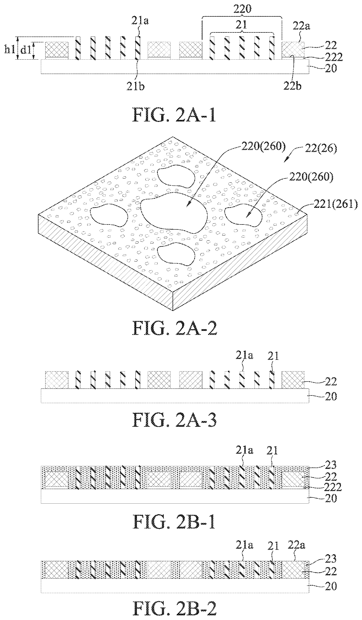
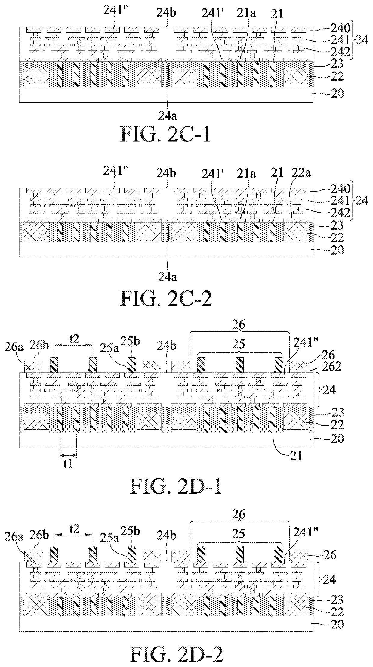
First, since the substrate still has the core layer, the conductive through holes are required, thus limiting the wiring density of the substrate.
Second, since the reinforcing plate is formed at a single side of the overall structure, the substrate is not symmetrical, thereby hindering its application in large-size packages.
Third, although the thickness of the reinforcing plate can be increased to
resist warping, such a method results in a longer conductive path (e.g., reference number 252), thereby increasing its processing difficulty. Further, the pitch is not easy to be minimized More seriously, the problem of reliability may occur. For example, due to the deep and long
conductive channel (e.g., reference number 250), a large amount of solder is required when an electronic element such as a chip is mounted to the substrate. Consequently, reliability problems such as voids and poor bonding may occur.
Fourth, the reinforcing plate is first coated with an insulating material. Due to the high-density holes (e.g., reference number 246), the
coating may be uneven or poor, causing a concern about occurrence of a
short circuit.
Therefore, how to overcome the above-described drawbacks of the prior art has become an urgent issue in the art.

