Gold-bumped interposer for vertically integrated semiconductor system

Inactive Publication Date: 2007-09-13
TEXAS INSTR INC
View PDF10 Cites 2 Cited by
  • Summary
  • Abstract
  • Description
  • Claims
  • Application Information

AI Technical Summary

Benefits of technology

[0007] Applicants recognize the need for a fresh concept of achieving a coherent, low-cost method of assembling high lead count, yet chip-scale and low contour devices; the concept includes substrates and packaging methods for stacking devices. The goal should be vertically integrated semiconductor systems, which may include integrated circuit chips of

Problems solved by technology

In known technology, however, the achievable bump pitch is limited.
These limits severely restrict the number of connections that can be made on the available chip surface, and thus constrain the use of flip-chip techniques, when devices with relatively small area chips are to be contacted.
Unchanged, however, is the traditional way of interconnecting the substrates to semiconductor chi

Method used


Image

  • Gold-bumped interposer for vertically integrated semiconductor system
  • Gold-bumped interposer for vertically integrated semiconductor system
  • Gold-bumped interposer for vertically integrated semiconductor system

Examples


Example

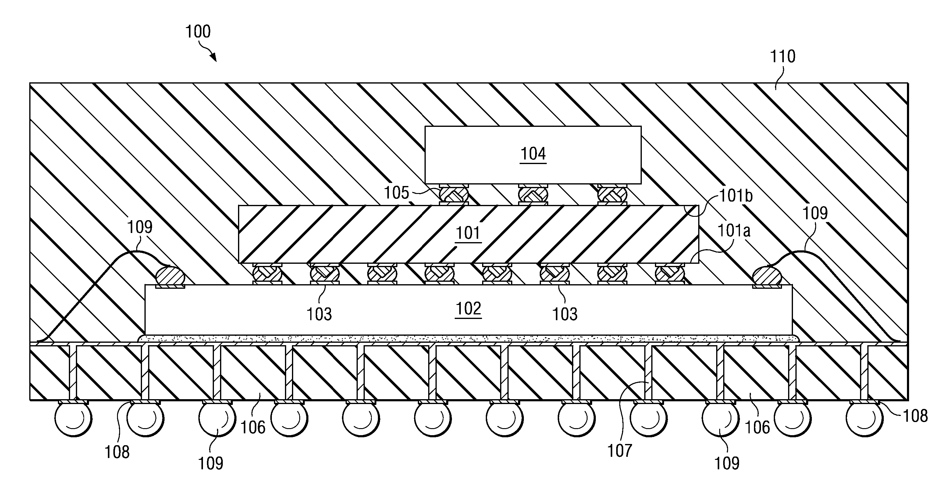
[0021]FIGS. 1 and 4 are examples of embodiments of the present invention, illustrating vertically integrated semiconductor systems, which are packaged in an encapsulation compound and, by means of solder bodies, prepared for connection to external parts. In FIG. 1, the system generally designated 100 has an interposer 101 made of an insulating body with first surface 101a and second surface 101b. Preferred materials for interposer 101 are ceramics or polymers in a sheet-like configuration; the polymers may be stiff or compliant. The interposers have typically a thickness in the range of about 50 to 500 μm.

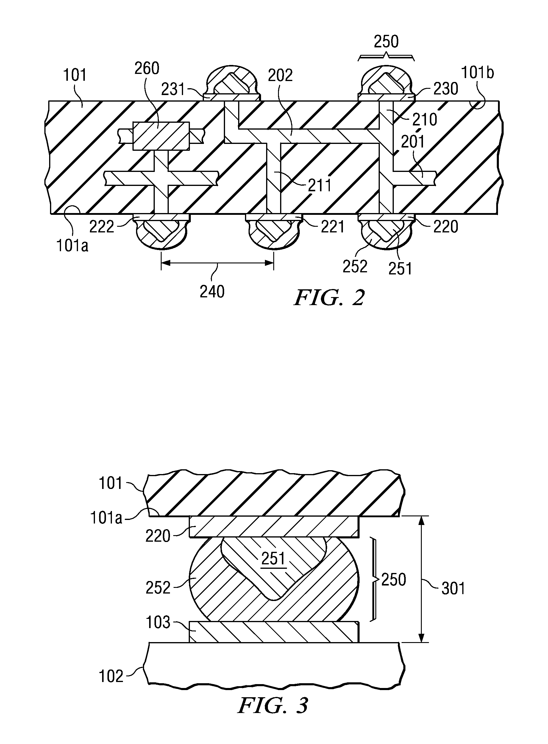
[0022] A portion of the interposer is magnified in FIG. 2 in order to show a plurality of electrically conductive lines 201, 202, etc., which are located between the first surface 101a and the second surface 101b of the interposer; the lines are patterned from sheets preferably made of copper or a copper alloy. The interposer further has a plurality of electrically conductive path...


PUM


Abstract

A semiconductor system (100) enabled by an interposer (101) with non-reflow metal studs (251), preferably gold, coated with reflow metals (252), preferably solder. The studs are on exit ports (220, 230, etc) of the interposer surface; selected exit ports may be spaced apart by less than 125 μm center to center. A first electrical device (102), such as one or more semiconductor chips with contact pads matching the locations of the interposer exit ports, contacts the studs on one interposer surface. A second electrical device (104), such as a semiconductor chip, a passive component, or both, is attached to the other interposer surface. A carrier (106) supports the first device and provides electrical connections (109) to external parts.

Description

FIELD OF THE INVENTION [0001] The present invention is related in general to the field of semiconductor devices and processes, and more specifically to structure and processes of low profile packages for vertically integrated semiconductor systems. DESCRIPTION OF THE RELATED ART [0002] The wide application of flip-chip assembly in the fabrication process flow of silicon integrated circuit (IC) devices is driven by several facts. First, the electrical performance of the semiconductor devices can be improved when the parasitic inductances correlated with conventional wire bonding interconnection techniques are reduced. Second, flip-chip assembly provides higher interconnection densities between chip and package than wire bonding. In particular, the absence of looped wires allows the reduction of package height (profile) in unison with thickness reductions of chips, leadframes, and encapsulations. Third, flip-chip assembly consumes less silicon “real estate” than wire bonding, and thus...

Claims


Application Information

Patent Timeline
IPC IPC(8): H01L23/02
CPCH01L23/49816H01L24/45H01L2924/10253H01L2224/73265H01L2224/48472H01L2224/32145H01L2924/01028H01L2924/01013H01L2924/01087H01L25/16H01L25/50H01L2224/16H01L2224/45144H01L2224/48145H01L2225/06506H01L2225/0651H01L2225/06517H01L2225/06572H01L2225/06586H01L2924/01004H01L2924/01012H01L2924/01014H01L2924/0102H01L2924/01046H01L2924/0105H01L2924/01078H01L2924/01079H01L2924/14H01L2924/15311H01L2924/19041H01L2924/20104H01L2924/20105H01L2924/20106H01L2924/20107H01L2924/30107H01L24/48H01L2924/01019H01L2924/00014H01L2924/00H01L24/05H01L2224/05147H01L2224/05568H01L2224/05573H01L2224/05644H01L2224/05655H01L2224/05664H01L2224/45015H01L2224/48465H01L2924/181H01L2924/00012
Inventor GERBER, MARK A.HUDDLESTON, WYATT A.
Owner TEXAS INSTR INC
Why Eureka
Try Eureka