Controlling Flip-Chip Techniques for Concurrent Ball Bonds in Semiconductor Devices

a technology of semiconductor devices and flip-chips, applied in semiconductor devices, semiconductor/solid-state device details, electrical apparatus, etc., can solve the problems of increasing the complexity of the product, the cost per functional unit should drop, and the increase of the functional complexity paralleled by the equivalent increase in the reliability of the product, so as to achieve excellent electrical performance, mechanical stability, and high product reliability.

Active Publication Date: 2007-10-04
TEXAS INSTR INC
View PDF10 Cites 37 Cited by
  • Summary
  • Abstract
  • Description
  • Claims
  • Application Information

AI Technical Summary

Benefits of technology

[0005]Applicants recognize the need for a fresh concept of achieving a coherent, low-cost method of shrinking semiconductor device packages both in two and in three dimensions, which includes device-stacking and package-on-package options for semiconductor devices as well as assembly options for flip-chip and wire bond interconnections. The device can be the base for a vertically integrated semiconductor system, which may include integrated circuit chips of functional diversity and passive components. The resulting system should have excellent electrical performance, mechanical stability, and high product reliability. Further, it will be a technical advantage that the fabrication method of the system is flexible enough to be applied for different semiconductor product families and a wide spectrum of design and process variations.

Problems solved by technology

First, the higher product complexity should largely be achieved by shrinking the feature sizes of the chip components while holding the package dimensions constant; preferably, even the packages should shrink.
Second, the increased functional complexity should be paralleled by an equivalent increase in reliability of the product.
Third, the cost per functional unit should drop with each generation of complexity so that the cost of the product with its doubled functionality would increase only slightly.
Recent applications especially for hand-held wireless equipments, combined with ambitious requirements for data volume and high processing speed, place new, stringent constraints on the size and volume of semiconductor components used for these applications.

Method used


Image

  • Controlling Flip-Chip Techniques for Concurrent Ball Bonds in Semiconductor Devices
  • Controlling Flip-Chip Techniques for Concurrent Ball Bonds in Semiconductor Devices
  • Controlling Flip-Chip Techniques for Concurrent Ball Bonds in Semiconductor Devices

Examples


Embodiment Construction

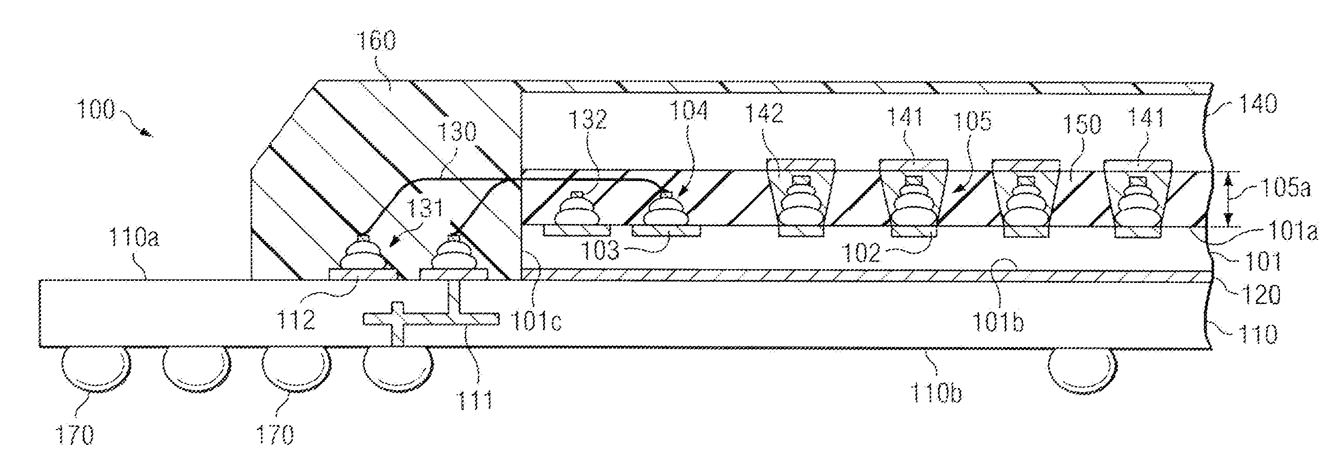
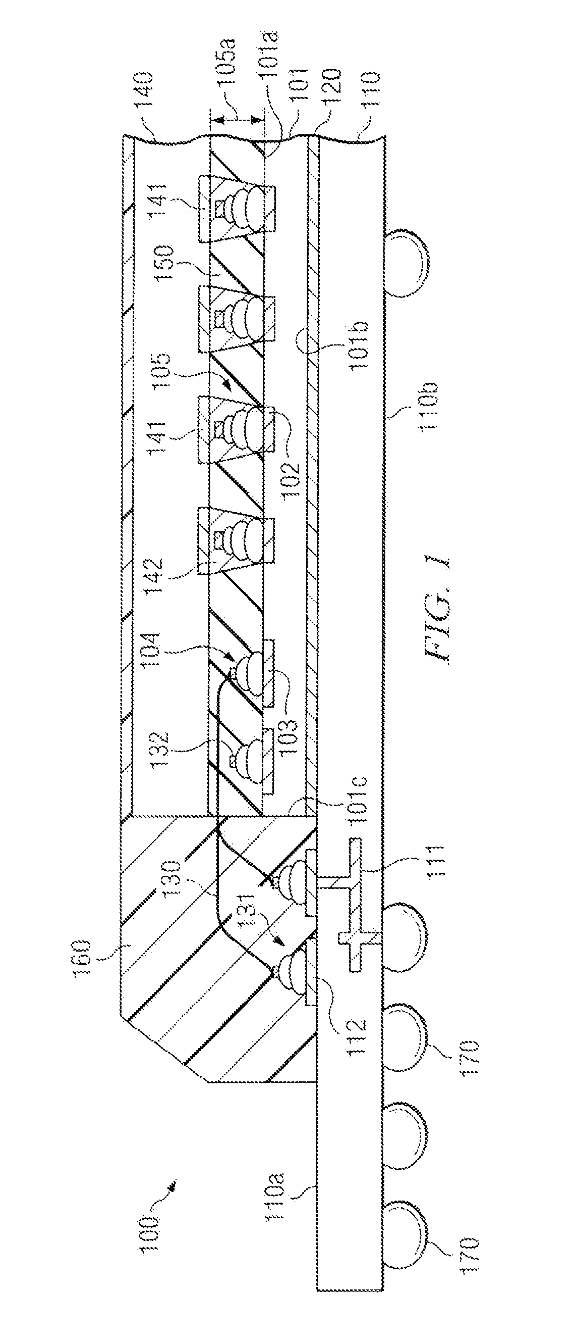
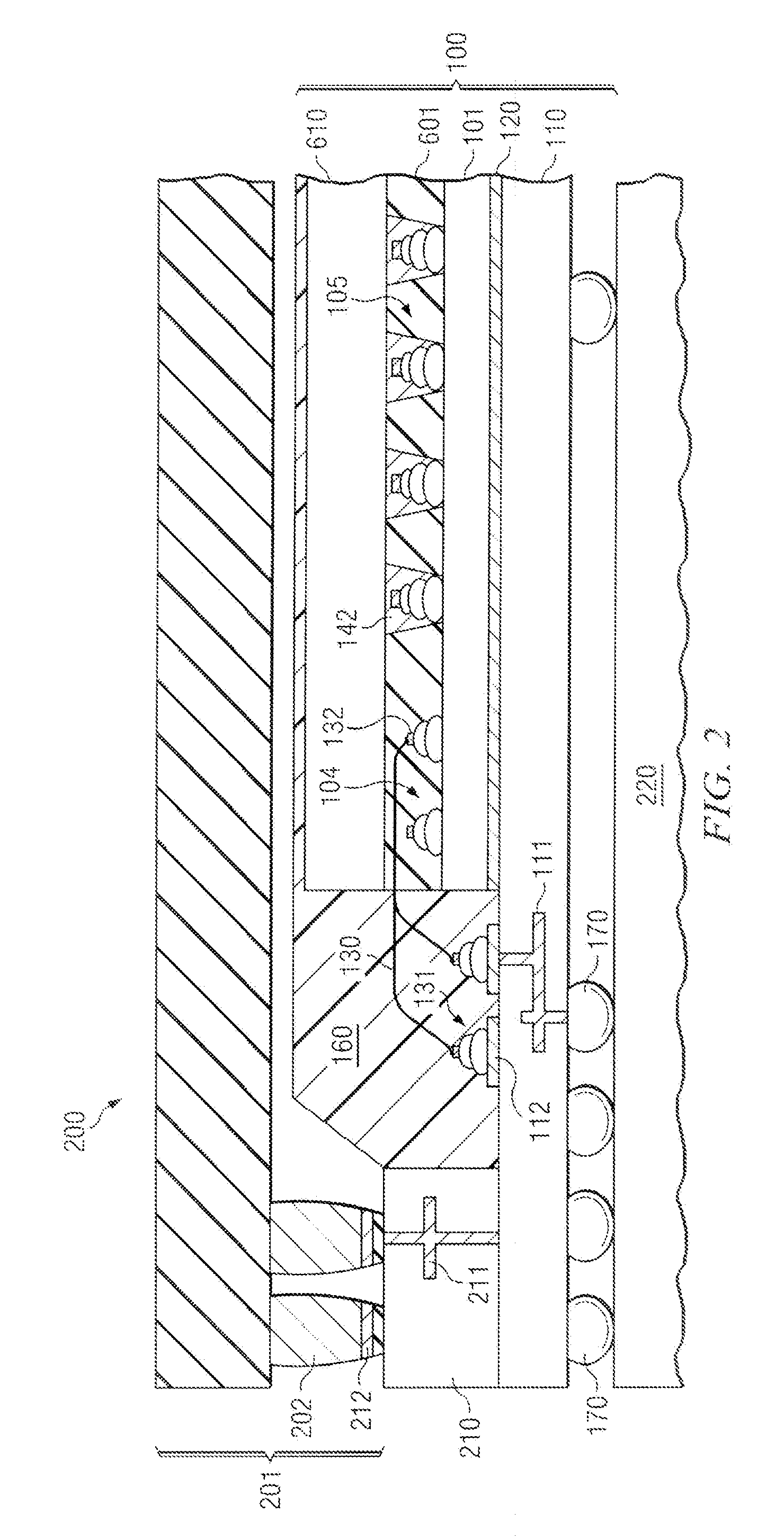
[0022]FIG. 1 illustrates a portion of an assembled semiconductor device, generally designated 100, which includes semiconductor chips stacked on a substrate by the invented combination of assembly techniques. The first semiconductor chip is designated 101; it has an active surface 101a, which includes the devices and circuits, a passive surface 101b, and a perimeter 101c. First chip 101 has a certain size, but FIG. 1 shows only the chip portion in the neighborhood of the chip perimeter. The active surface of first chip 101 has a first set of contact pads 102 located in the interior portion of the chip, and a second set of contact pads 103 located in the peripheral portion of the chip.

[0023]As depicted in FIG. 1, the contact pads 103 of the second set have a deformed sphere 104 of non-reflow metal placed on the contact pads. The contact pads 102 of the first set have more than one deformed sphere placed on the contact pad so that the spheres form column-shaped spacers 105 with a cert...


PUM


Abstract

A device has a first semiconductor chip (101) with contact pads in an interior first set (102) and a peripheral second set (103). A deformed sphere (104) of non-reflow metal such as gold is placed on each contact pad of the first and second sets. At least one additional deformed sphere (105) is placed on the first set pads, forming column-shaped spacers. The first chip is attached to a substrate (110) with a chip attachment location and a third set of contact pads (112) near the location. Low profile bond wires (130) span between the pads of the third set and the second set. A second semiconductor chip (140) of a size has a fourth set of contact pads (141) at locations matching the first set pads. The second chip is placed over the first chip so that the fourth set pads are aligned with the spacers on the matching first set pads, and at least one edge of the second chip overhangs the sphere on at least one pad of the second set. A reflow metal (142) bonds the spacers to the second chip, while the spacers space the first and second chips by a gap (105a) wide enough for placing the wire spans to the second set pads.

Description

FIELD OF THE INVENTION[0001]The present invention is related in general to the field of semiconductor devices and processes, and more specifically to structure and processes of low profile packages for vertically integrated semiconductor systems.DESCRIPTION OF THE RELATED ART[0002]The long-term trend in semiconductor technology to double the functional complexity of its products every 18 months (Moore's “law”) has several implicit consequences. First, the higher product complexity should largely be achieved by shrinking the feature sizes of the chip components while holding the package dimensions constant; preferably, even the packages should shrink. Second, the increased functional complexity should be paralleled by an equivalent increase in reliability of the product. Third, the cost per functional unit should drop with each generation of complexity so that the cost of the product with its doubled functionality would increase only slightly.[0003]As for the challenges in semiconduc...

Claims


Application Information

Patent Timeline
Patent Type & Authority Applications(United States)
IPC IPC(8): H01L23/485H01L21/60
CPCH01L21/563H01L23/3128H01L24/05H01L24/11H01L24/45H01L24/48H01L24/73H01L24/81H01L24/85H01L24/97H01L25/0657H01L2224/0401H01L2224/04042H01L2224/05624H01L2224/05647H01L2224/1134H01L2224/1308H01L2224/13099H01L2224/13139H01L2224/13144H01L2224/13147H01L2224/16145H01L2224/45015H01L2224/45144H01L2224/48227H01L2224/4845H01L2224/48471H01L2224/48624H01L2224/48647H01L2224/73203H01L2224/73207H01L2224/73265H01L2224/8121H01L2224/81815H01L2224/85045H01L2224/97H01L2225/0651H01L2225/06513H01L2225/06579H01L2924/01005H01L2924/01013H01L2924/01014H01L2924/01027H01L2924/01028H01L2924/01029H01L2924/01031H01L2924/01032H01L2924/01047H01L2924/0105H01L2924/01079H01L2924/01082H01L2924/01083H01L2924/014H01L2924/05042H01L2924/14H01L2924/15311H01L2924/20105H01L2924/20106H01L2924/20107H01L2924/20751H01L2924/20752H01L2924/20753H01L2924/20754H01L2924/20755H01L2924/20756H01L2924/20757H01L2924/20758H01L2924/20759H01L24/13H01L2224/32225H01L2924/01006H01L2924/01033H01L2924/00014H01L2924/00H01L2924/00012
Inventor WALTER, DAVID N.LE, DUY-LOAN T.GERBER, MARK A.
Owner TEXAS INSTR INC
Why Eureka
Try Eureka