Method of spacer-defined direct patterning in semiconductor fabrication

a technology of direct patterning and semiconductors, applied in photomechanical treatment, instruments, electrical equipment, etc., can solve the problems of line-to-line short circuit, the limit of miniaturization by sddp, and the surface roughness of approximately 5 nm, so as to reduce the variability of microfabrication

Active Publication Date: 2019-08-22
ASM IP HLDG BV
View PDF4 Cites 226 Cited by
  • Summary
  • Abstract
  • Description
  • Claims
  • Application Information

AI Technical Summary

Benefits of technology

[0005]In some embodiments, variations in microfabrication can be reduced by providing a template having a resist patterned by EUV lithography; conducting trimming or etching of the resist using a plasma-enhanced atomic layer deposition (PEALD) apparatus; and depositing a S...

Problems solved by technology

However, there is a limit of miniaturization by SDDP due to limited exposure accuracy, and also, the prospect of actually using EUV lithography has recently emerged.
EUV lithography enables patterning with a pattern dimension of 10 to 20 nm (the minimum dimension in ArF laser lithography is approximately 40 nm); however, patterning accuracy, which is surface roughness evaluate...

Method used


Image

  • Method of spacer-defined direct patterning in semiconductor fabrication
  • Method of spacer-defined direct patterning in semiconductor fabrication
  • Method of spacer-defined direct patterning in semiconductor fabrication

Examples


example 1

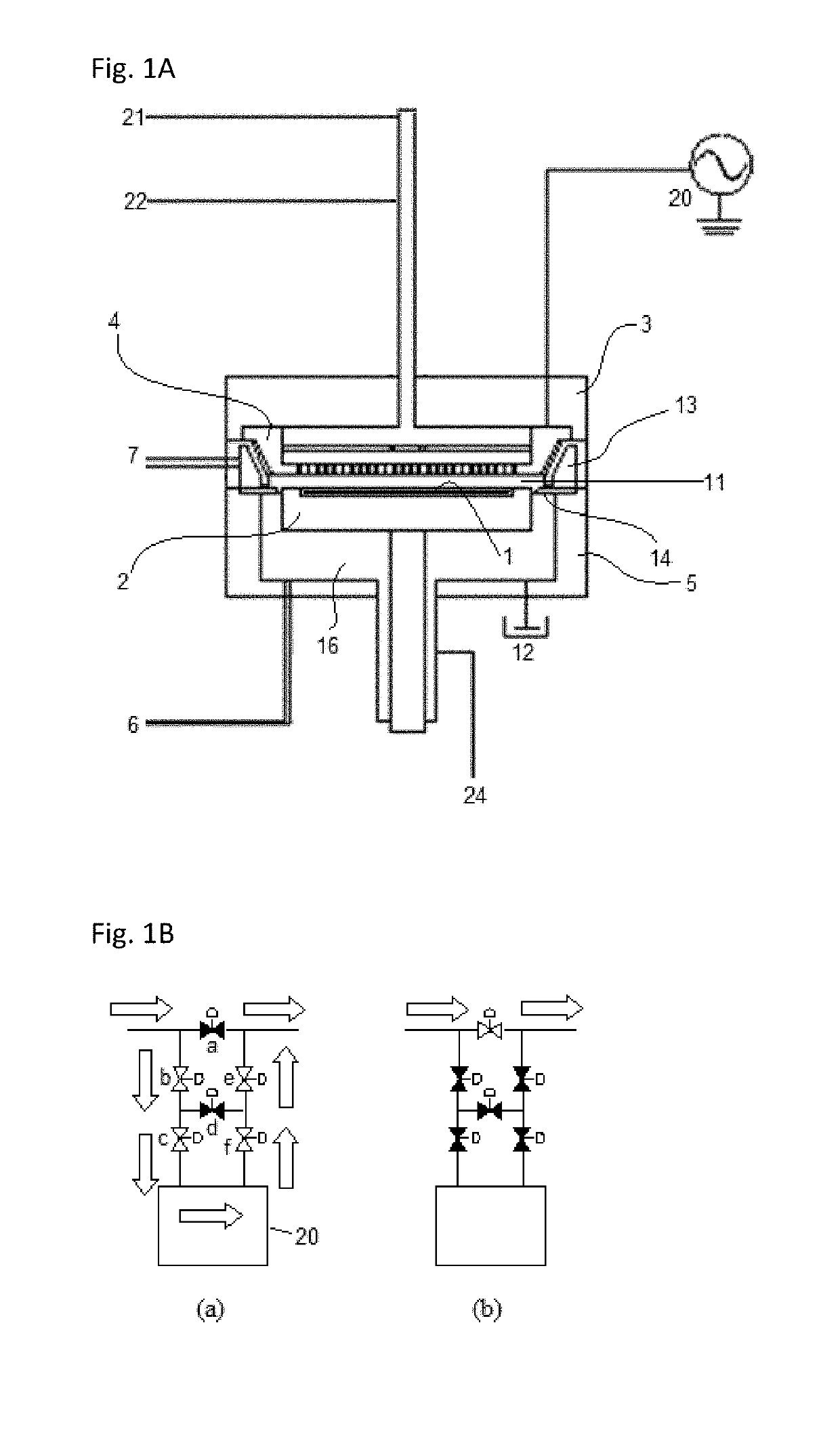
[0072]A photoresist pattern (constituted by e.g., Novolacs designed for EUV lithography) formed on a SiOC layer of a 300-mm substrate and having an initial CD of about 35 nm was subjected to trimming using a PEALD apparatus illustrated in FIG. 1A under conditions shown in Table 4 below.

TABLE 4(numbers are approximate)Conditions for trimmingResist materialEUV resistTemperature75°C.Pressure200PaEtchantO2Etchant flow1SLMRF power for a 300-mm wafer30WDurationVaried (see FIG. 2)Trimming rate in width direction1.4nm / secTrimming rate in height direction2nm / sec

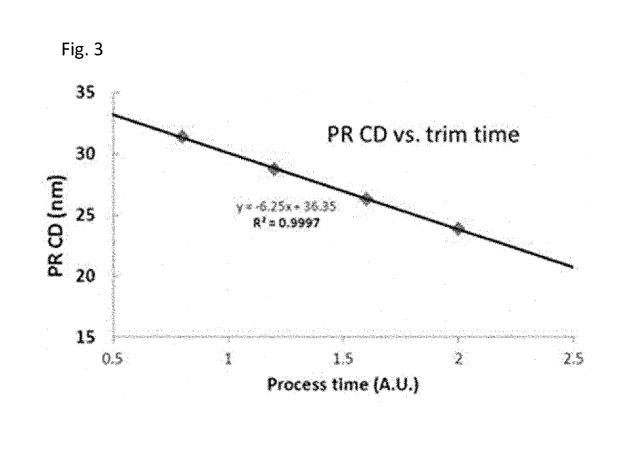
[0073]FIG. 3 is a graph showing the relationship between CD of the photoresist (“PR CD”) and process times of trimming (“Process time”). It is confirmed that CD of the photoresist was reduced linearly as a function of process time of trimming at least to the degree that CD was as low as about 20 nm.

example 2

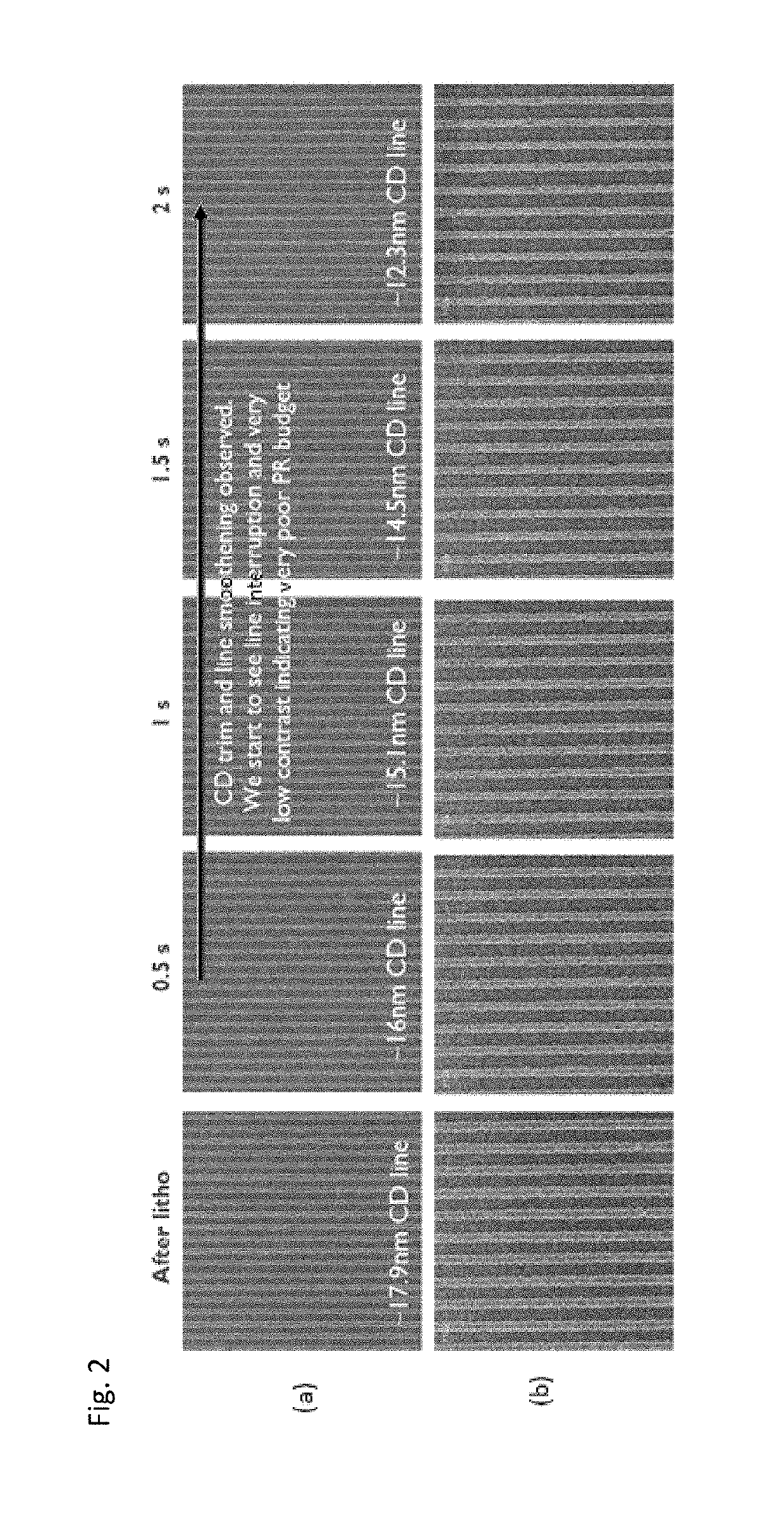
[0074]Even though EUV lithography has higher exposure accuracy than ArF laser, it is difficult to reduce the CD (Critical Dimension) of a resist pattern to the degree which is as low as 12 nm or lower. In this example, a photoresist was subjected to trimming in a manner substantially similar to that in Example 1 except that the initial CD of the photoresist was about 17.9 nm. FIG. 2 shows SEM photographs of patterned surfaces after EUV lithography without trimming (“After litho”), after 0.5 seconds of trimming (“0.5 s”), after 1.0 seconds of trimming (“1 s”), after 1.5 seconds of trimming (“1.5 s”), and after 2.0 seconds of trimming (“2 s”), wherein the lower photos (b) are taken at a higher magnification than that for the upper photos (a).

[0075]As can be seen in FIG. 2, as trimming of the resist pattern progressed, the CD of the resist pattern was reduced from about 17.9 nm (without trimming), about 16 nm (0.5 sec. of trimming), about 15.1 nm (1 sec. of trimming), about 14.5 nm (1....

example 3

[0076]In this example, a photoresist (ArF resist with an initial CD of about 7.90 nm (mean)) was subjected to trimming in a manner similar to that in Example 1 under the conditions shown in Table 5 below.

TABLE 5(numbers are approximate)Conditions for trimmingResist materialArF resistTemperature75°C.Pressure200PaEtchantO2Etchant flow2SLMRF power for a 300-mm wafer30WDuration13.2secondsTrimming rate in width direction0.93nm / secTrimming rate in height directionNot measured

[0077]The trimmed resist pattern was then subjected to SiO2 deposition by PEALD which was conducted under the conditions shown in Table 6 below.

TABLE 6(numbers are approximate)Conditions for PEALDSubstrate temperature75°C.Electrode gap (a thickness of a substrate is10mmabout 0.7 mm)Pressure500PaPrecursorBDEASCarrier gas / Dilution gasArFlow rate of carrier gas (continuous)1000sccmFlow rate of dilution gas (continuous)1000sccmFlow rate of precursorCorresponding to the flowrate of carrier gasRF power (13.56 MHz) for a 300...


PUM


Abstract

A method of spacer-defined direct patterning in semiconductor fabrication includes: providing a photoresist structure having a target width of lines; trimming the photoresist structures such that a width of each trimmed photoresist structure is smaller than the target width; depositing an oxide film on the template, thereby entirely covering with the oxide film an exposed top surface of the template and the trimmed photoresist structures; etching the oxide film-covered template to remove an unwanted portion of the oxide film without removing the trimmed photoresist structures so as to form vertical spacers isolated from each other, each spacer substantially maintaining the target width and being constituted by the trimmed photoresist structures and a vertical portion of the oxide film covering sidewalls of the trimmed photoresist structures; and etching the spacer-formed template to transfer a pattern constituted by the spacers to the template.

Description

BACKGROUND OF THE INVENTIONField of the Invention[0001]The present invention generally relates to a method of patterning in semiconductor fabrication, particularly a method of spacer-defined direct patterning in semiconductor fabrication using, e.g., EUV (Extreme Ultra Violet) for photolithography.Description of the Related Art[0002]To correspond to miniaturization of semiconductor devices, a reduction of wavelength of light source for photolithography progresses, e.g., changing from ArF (Argon Fluoride laser) to EUV. Heretofore, due to low productivity of EUV lithography as discussed below, miniaturization of semiconductor devices has been achieved by using spacer-defined double patterning (SDDP). However, there is a limit of miniaturization by SDDP due to limited exposure accuracy, and also, the prospect of actually using EUV lithography has recently emerged. Accordingly, it is expected that direct patterning using EUV lithography will be placed into practical use in semiconductor...

Claims


Application Information

Patent Timeline
IPC IPC(8): H01L21/033H01L21/311H01L21/027H01L21/02
CPCH01L21/0338H01L21/31138H01L21/0276H01L21/0337H01L21/0332H01L21/31116H01L21/02164H01L21/02274H01L21/0228H01L21/0275H01L21/0274H01L21/02219H01L21/32137H01L21/0273H01L21/02554G03F7/2004G03F7/70033G03F7/091G03F7/70875H01L21/76832H01L21/31144H01L21/027H01L21/76816
Inventor NOZAWA, TOSHIHISAISHIKAWA, DAIKUBOTA, TOMOHIRO
Owner ASM IP HLDG BV
Why Eureka
Try Eureka