Semiconductor device and semiconductor device manufacturing method

a semiconductor device and semiconductor technology, applied in semiconductor devices, diodes, electrical devices, etc., can solve the problems of reducing the withstand voltage of the n-type drift layer, affecting the withstand voltage of the manufactured products, so as to achieve the effect of reducing the withstand voltag

Active Publication Date: 2019-08-22
LAPIS SEMICON CO LTD
View PDF5 Cites 6 Cited by
  • Summary
  • Abstract
  • Description
  • Claims
  • Application Information

AI Technical Summary

Benefits of technology

[0012]According to the above aspects, the present disclosure provides, in a semiconductor device having field plates, a semiconductor device and a semiconductor device manufacturing method that may suppress a decrease in the withstand voltage due to electric field concentration at the trench bottom portions.

Problems solved by technology

As a result, the depletion layer broadens from the side walls of the trench, and the interior of the N type drift layer is completely depleted.
As a result, it is difficult to control the impurity concentration at the N type low concentration regions that controls the extending of the depletion layer, and thus, the withstand voltages in the manufactured products may vary (reproducibility of the withstand voltage being low).
On the other hand, in the semiconductor device according to JP-A No. 2013-214551, in a case in which drain voltage is applied, it is easy for an electric field to concentrate at the trench bottom portion, and, if the voltage specifications are high, it is difficult to obtain the desired withstand voltage.
Namely, it is easy for electric field concentration to arise at the trench bottom portion, and breakdown may occur.

Method used


Image

  • Semiconductor device and semiconductor device manufacturing method
  • Semiconductor device and semiconductor device manufacturing method
  • Semiconductor device and semiconductor device manufacturing method

Examples


first exemplary embodiment

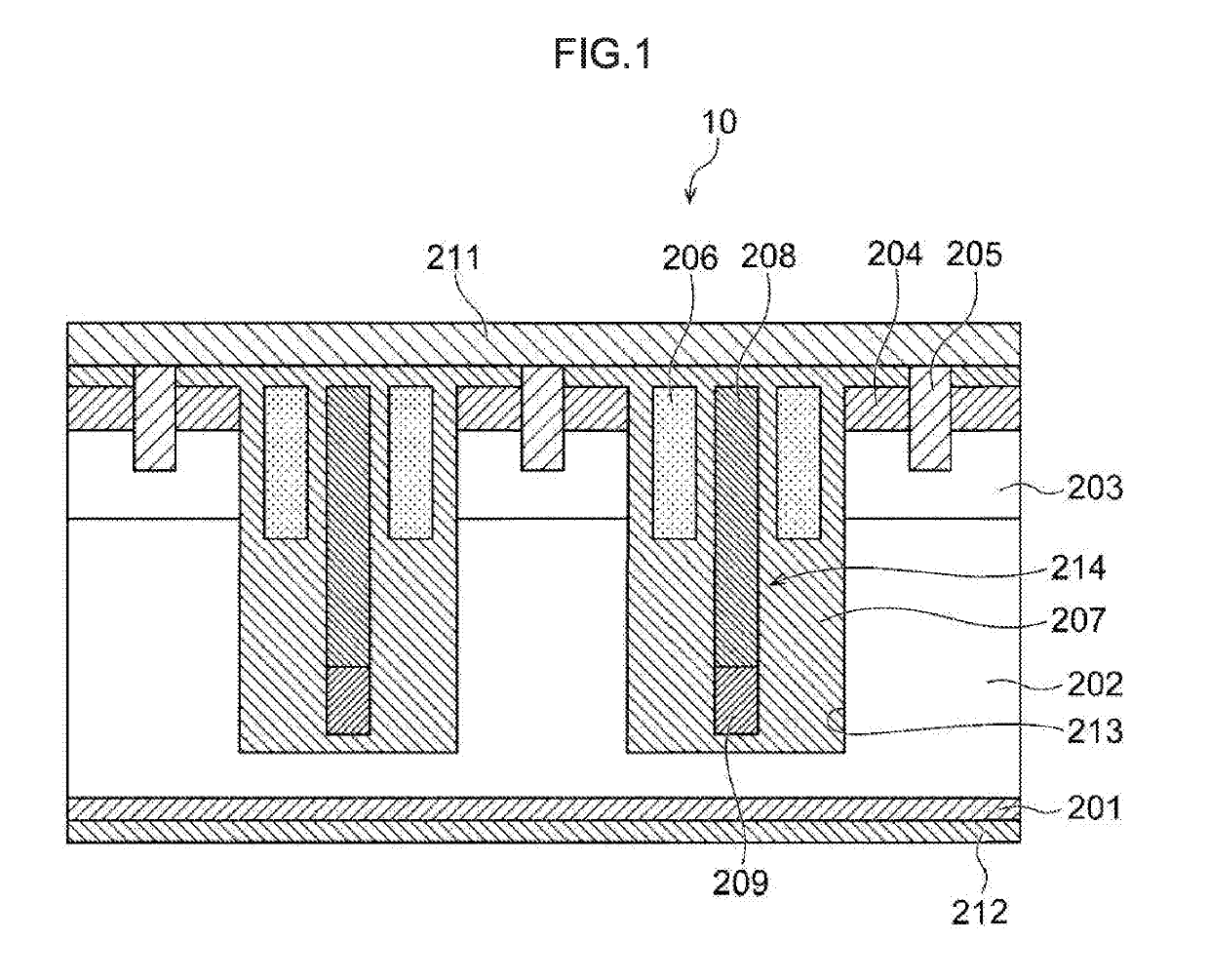
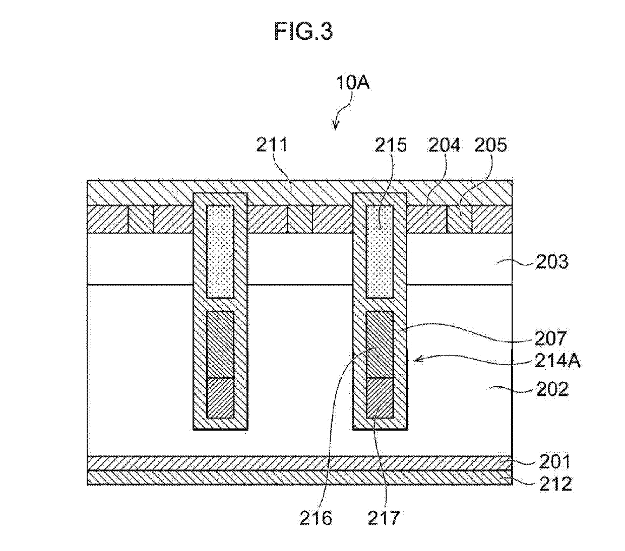
[0024]A semiconductor device 10 according to the present exemplary embodiment is described with reference to FIG. 1 and FIG. 2. In the present exemplary embodiment, an N type silicon substrate (see FIG. 2) is used as an example of the substrate. As shown in FIG. 1, the semiconductor device 10 includes a drain electrode 212, an N+ type drain layer 201, an N− type drift layer 202, a P type body layer 203, an N+ type source layer 204, contact electrodes 205, gate electrodes 206, an insulating film 207, P type field plates 208, N type field plates 209, and a source electrode 211. The source electrode 211 is connected to the N+ type source layer 204 via the contact electrodes 205. The drain electrode 212 is connected to the N+ type drain layer 201. Namely, the semiconductor device 10 is structured as a vertical type MOS FET (Field Effect Transistor) having a vertical type field plate structure. Note that the “+” that is added to the N means that the impurity concentration is higher than ...

second exemplary embodiment

[0046]A semiconductor device 10B according to the present exemplary embodiment is described with reference to FIG. 4 and FIG. 5. In the semiconductor device 10B, two of each of the P type field plates and the N type field plates are disposed. Accordingly, structures that are similar to those of the semiconductor device 10 are denoted by the same reference numerals, and detailed description thereof is omitted.

[0047]As shown in FIG. 4, the semiconductor device 10B has P type field plates 208-1, 208-2 and N type field plates 209-1, 209-2. A field plate 214B is structured by the P type field plates 208-1, 208-2 and the N type field plates 209-1, 209-2.

[0048]In the above-described semiconductor device 10, one PN junction is provided in order to lower the end portion of the field plate. However, in the semiconductor device 10B according to the present exemplary embodiment, two PN junctions are provided. Namely, a repeating structure of N type, P type, N type, P type is provided from the e...

third exemplary embodiment

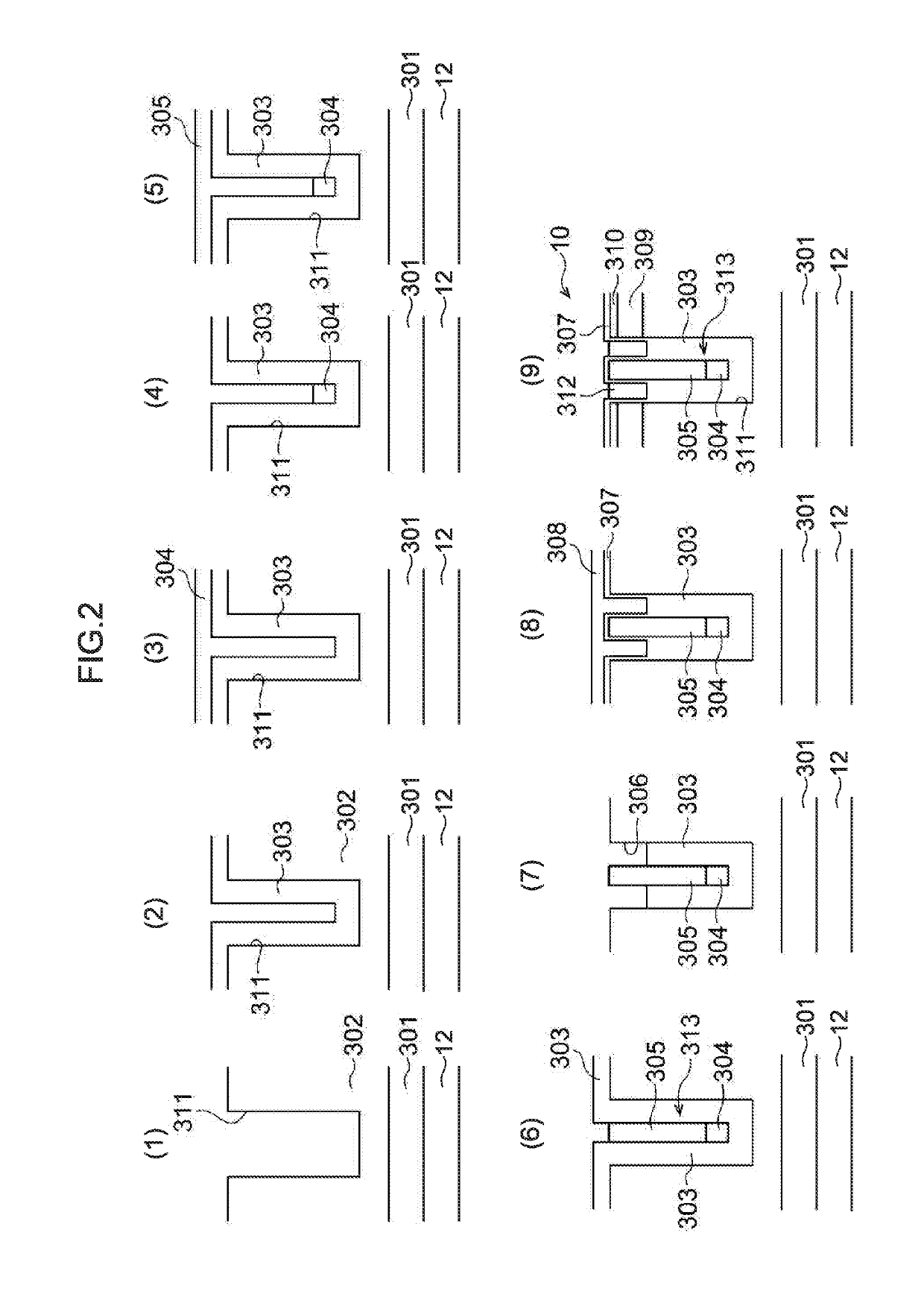
[0059]A semiconductor device 10C and a semiconductor device manufacturing method 10C according to the present exemplary embodiment are described with reference to FIG. 6. The present exemplary embodiment uses ion implantation in the formation of the PN diodes.

[0060]The steps of the formation of an N+ type drain layer 601, an N− type drift layer 602 and trenches 608, the formation of an insulating film 603, and up through the filling of polysilicon 604, are similar to those of (1) through (3) of FIG. 5 ((1) of FIG. 6).

[0061]Next, the polysilicon 604 is etched-back to the same position as the surface (the main surface) of the semiconductor substrate 12 ((2) of FIG. 6).

[0062]Next, portions other than the field plate formation portions are protected by a photoresist 605 ((3) of FIG. 6).

[0063]Via the photoresist 605, P type impurities and N type impurities are implanted with the energy amounts thereof being varied, and plural PN diodes are built into the positions that will become the en...


PUM


Abstract

A semiconductor device including: a first semiconductor layer having a first conductive type; a second semiconductor layer provided on the first semiconductor layer, the second semiconductor layer having a second conductive type that is a conductive type different from the first conductive type; an impurity region of the first conductive type formed at a surface of the second semiconductor layer; first electrodes contacting the impurity region, the second semiconductor layer, and the first semiconductor layer via a first insulating film; and second electrodes contacting the first electrodes via a second insulating film, and contacting the first semiconductor layer via a third insulating film, the second electrodes including PN junctions at borders between upper portions that contact the first semiconductor layer via the third insulating film and lower portions that contact the first semiconductor layer via the third insulating film.

Description

CROSS-REFERENCE TO RELATED APPLICATION[0001]This application claims priority under 35 USC 119 from Japanese Patent Application No. 2018-029528, filed on Feb. 22, 2018, the disclosure of which is incorporated by reference herein.BACKGROUNDTechnical Field[0002]The present disclosure relates to a semiconductor device and a semiconductor device manufacturing method, and in particular, to a high voltage semiconductor device and a high voltage semiconductor device manufacturing method.Related Art[0003]In a high voltage semiconductor device, improvement in the withstand voltage and a decrease in the ON resistance are required. An embedded field plate structure has been proposed as a method for realizing an increase in the withstand voltage and a lowering of the ON resistance of a high voltage semiconductor device. In an embedded field plate structure, trenches are provided in the drift layer, the potential of the field plates embedded within the trenches is fixed, and, by extending the dep...

Claims


Application Information

Patent Timeline
Patent Type & Authority Applications(United States)
IPC IPC(8): H01L29/78H01L29/40H01L29/417H01L29/66H01L21/266
CPCH01L29/7813H01L29/407H01L29/7804H01L29/41741H01L29/66712H01L21/266H01L29/66734H01L29/4236H01L29/41766
Inventor YAMANOBE, TOMOMITAKESHITA, YOSHINOBUKODAMA, KAZUTAKAORITU, MINAKO
Owner LAPIS SEMICON CO LTD
Why Eureka
Try Eureka