Insulated gate semiconductor device and method of manufacturing same

a technology of insulated gate and semiconductor, which is applied in the direction of semiconductor devices, diodes, electrical equipment, etc., can solve the problems of weak electric field strength and electric fields to be applied to polysilicon, and achieve the effects of reducing bipolar operation of body diodes, low resistance, and high withstand voltag

Active Publication Date: 2019-09-19
FUJI ELECTRIC CO LTD
View PDF2 Cites 8 Cited by
  • Summary
  • Abstract
  • Description
  • Claims
  • Application Information

AI Technical Summary

Benefits of technology

[0012]The present invention makes it possible to provide an insulated gate semiconductor device and a method of manufacturing the same

Problems solved by technology

However, in Patent Document 1, the polysilicon forming the barrier-forming layer is exposed to the drift region due to being in contact

Method used


Image

  • Insulated gate semiconductor device and method of manufacturing same
  • Insulated gate semiconductor device and method of manufacturing same
  • Insulated gate semiconductor device and method of manufacturing same

Examples


embodiment 1

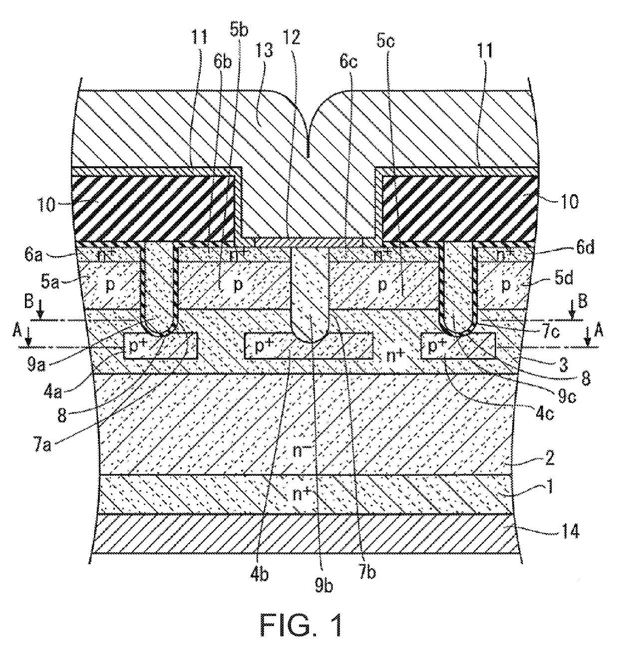
[0044]As shown in FIG. 1, an insulated gate semiconductor device (MISFET) according to Embodiment 1 of the present invention includes a first conductivity type (n-type) charge transport region (2, 3) that transports majority carriers. The charge transport region (2, 3) is made of a two-layer structure of an n− drift layer2 and an n-type current spreading layer (CSL) 3 disposed on the drift layer 2. The drift layer 2 is a semiconductor region capable of transporting the majority carriers injected into the drift layer 2 via a drift electric field. Depending on the design specifications, the current spreading layer 3 need not be provided on the drift layer 2. The impurity concentration of the drift layer 2 is, for example, not less than about 1×1015 cm−3 and not more than about 1×1018 cm−3, and the impurity concentration of the current spreading layer 3 is, for example, not less than about 5×1016 cm−3 and not more than about 5×1017 cm−3.

[0045]Injection control regions (base regions) 5a...

embodiment 2

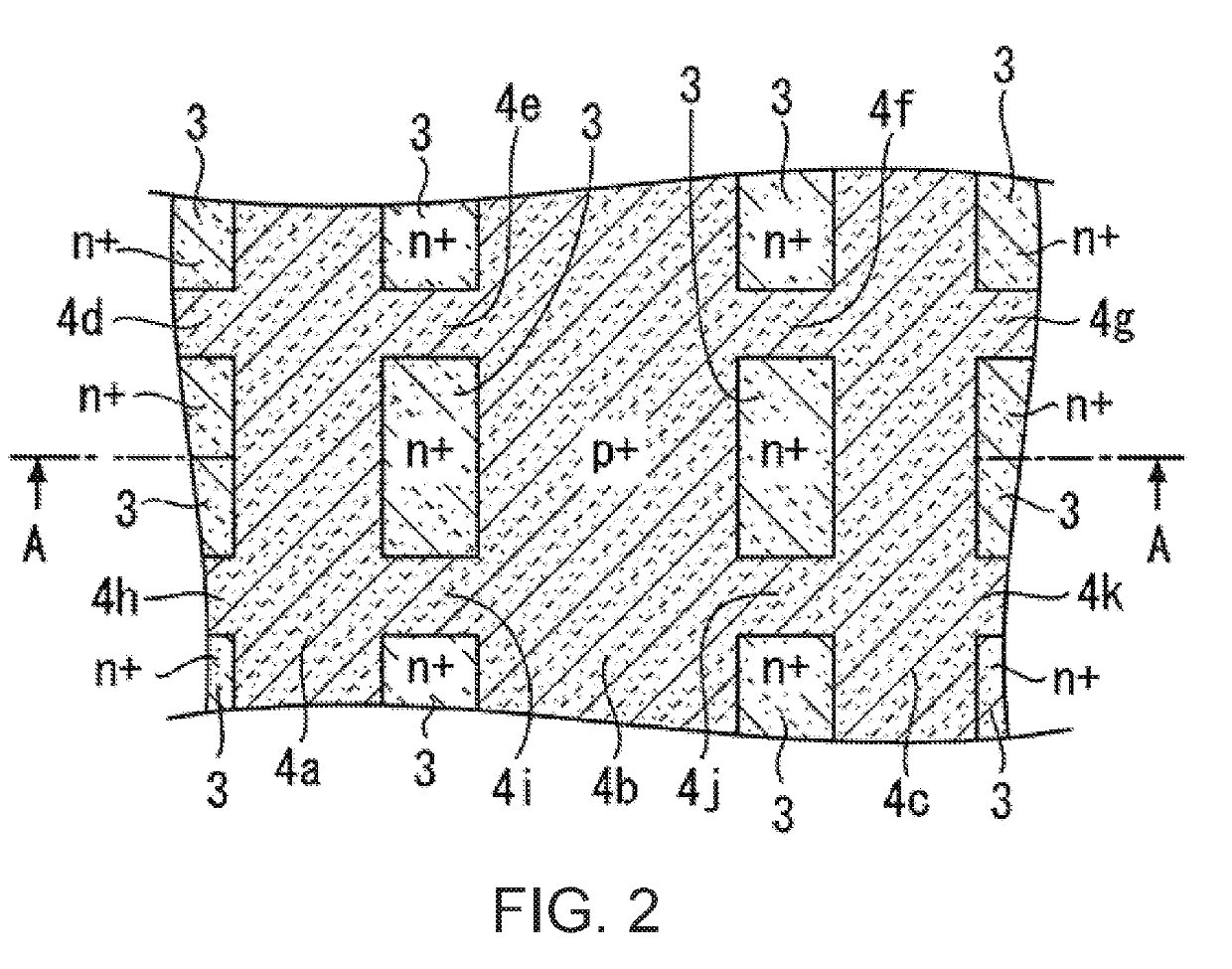
[0085]An insulated gate semiconductor device according to Embodiment 2 of the present invention differs from the insulated gate semiconductor device according to Embodiment 1 shown in FIG. 1 etc. in that, in the cross-sectional structure shown in FIG. 18, the contact protection region 4b contacting the bottom surface of the injection suppression region 9b, and the gate protection regions 4a, 4c contacting the bottom surface of the gate electrodes 9a, 9c are continuous with one another and form a uniform layer.

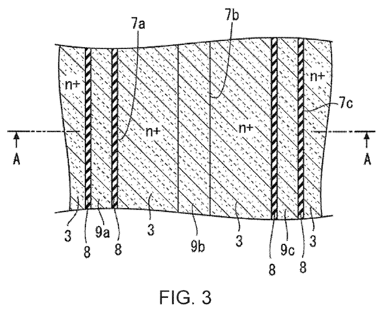
[0086]FIG. 19 shows a planar layout seen from the A-A direction horizontally cutting through the uniform layer where the gate protection regions 4a, 4c and contact protection region 4b are continuous with one another in FIG. 18. The cross-sectional view in the vertical direction seen from the A-A direction of FIG. 19 corresponds to FIG. 18. As shown in FIG. 19, the gate protection regions 4a, 4c extend in parallel to each other as stripe-shaped patterns extending in the vertica...

embodiment 3

[0091]As shown in FIG. 21, the insulated gate semiconductor device according to Embodiment 3 of the present invention differs from the insulated gate semiconductor device according to Embodiment 1 in further including cover regions 15a, 15b provided between the injection suppression region 9b and injection control regions 5b, 5c in a sheath shape surrounding the injection suppression region 9b. The cover regions 15a, 15b are made of second conductivity type (p−) SiC of a lower concentration than the injection control regions 5b, 5c. The other configurations of the insulated gate semiconductor device according to Embodiment 3 are the same as the insulated gate semiconductor device according to Embodiment 1.

[0092]In the insulated gate semiconductor device according to Embodiment 1 shown in FIG. 1, the width of the injection suppression region 9b is narrow, and thus the current path narrows and resistance increases. In contrast, in the insulated gate semiconductor device according to E...


PUM


Abstract

Provided are: injection control regions of a second conductivity type provided on a charge transport region of a first conductivity type; main electrode regions of the first conductivity type provided on the injection control regions; insulated gate electrode structures going through the main electrode region and the injection control regions in the depth direction; an injection suppression region going through the main electrode regions and the injection control regions in the depth direction so as to form a pn junction in a path leading to the charge transport region, the injection suppression region including a semiconductor material with a narrower bandgap than a material of the charge transport region; and a contact protection region of the second conductivity type contacting the bottom surface of the injection suppression region.

Description

BACKGROUND OF THE INVENTIONTechnical Field[0001]The present invention relates to an insulated gate semiconductor device having a trench gate structure and a method of manufacturing the same.Background Art[0002]A vertical MIS field effect transistor (FET) has a built-in parasitic pn diode (body diode) formed of an n-type drift region and a p-type base region. In the case of a MISFET (SiC-MISFET) using silicon carbide (SiC) as the material, the built-in potential of the body diode is higher than if silicon were used as the material, and thus ON resistance becomes higher and loss increases. Furthermore, when the body diode is ON and conductive, characteristic degradation occurs due to the bipolar operation of the body diode, thus decreasing reliability.[0003]In order to suppress the bipolar operation of the body diode of the SiC-MISFET, a structure has been proposed in which the MIS transistor structure includes a barrier-forming layer that forms, by being in contact with the drift reg...

Claims


Application Information

Patent Timeline
IPC IPC(8): H01L29/78H01L29/423H01L29/10H01L29/16H01L29/08H01L29/66
CPCH01L29/7804H01L29/7813H01L29/0852H01L29/1095H01L29/4236H01L29/66734H01L29/1608H01L29/66068H01L29/0878H01L29/0623H01L29/0696H01L29/165H01L29/7805H01L29/7397H01L29/7392
Inventor KINOSHITA, AKIMASA
Owner FUJI ELECTRIC CO LTD
Why Eureka
Try Eureka