Methods And Systems For Real Time Measurement Control

a measurement control and real-time technology, applied in the field of metalrology systems and methods, can solve the problems of difficult optical radiation penetration to the bottom layer, difficult characterization, and increased difficulty in characterization, so as to reduce the effect of surface roughness

Active Publication Date: 2019-09-26
KLA CORP
View PDF17 Cites 9 Cited by
  • Summary
  • Abstract
  • Description
  • Claims
  • Application Information

AI Technical Summary

Benefits of technology

[0019]In some embodiments, measurement recipe optimization is controlled to trade off measurement robustness and measurement time. This enables flexibility in the case of outliers and process excursions.
[0021]In some embodiments, measurement recipe optimization is controlled to minimize any combination of measurement uncertainty, measurement time, move time, and target dose. In some of these embodiments, measurement recipe optimization is controlled to minimize the sum of measurement time and move time for a sequence of collections.
[0027]In a further aspect, the measurement quality and performance of the metrology system is controlled based on a measured zero order beam. In some examples, the estimates of measurement quality and performance described hereinbefore are provided as input to a feedback controller. The feedback controller communicates control commands that result in changes in state of one or more elements of the metrology system that improves measurement system quality and performance.
[0029]In some examples, the control commands are provided to one or more positioning devices that control the location of one or more optical elements of the metrology system. In response, the one or more positioning devices changes a position / orientation of one or more optical elements to adjust the incidence angles, focal distance between the illumination source and illumination optics, beam positioning, location of the beam spot on the optic to minimize the effects of surface roughness, etc.

Problems solved by technology

As devices (e.g., logic and memory devices) move toward smaller nanometer-scale dimensions, characterization becomes more difficult.
Devices incorporating complex three-dimensional geometry and materials with diverse physical properties contribute to characterization difficulty.
For example, modern memory structures are often high-aspect ratio, three-dimensional structures that make it difficult for optical radiation to penetrate to the bottom layers.
Optical metrology tools utilizing infrared to visible light can penetrate many layers of translucent materials, but longer wavelengths that provide good depth of penetration do not provide sufficient sensitivity to small anomalies.
As a result, the parameters characterizing the target often cannot be reliably decoupled.
However, the mirror like structure of 3D FLASH intrinsically causes decreasing light intensity as the illumination propagates deeper into the film stack.
This causes sensitivity loss and correlation issues at depth.
In this scenario, SCD is only able to successfully extract a reduced set of metrology dimensions with high sensitivity and low correlation.
Optical radiation is often unable to penetrate layers constructed of these materials.
As a result, measurements with thin-film scatterometry tools such as ellipsometers or reflectometers are becoming increasingly challenging.
Although state of the art optical and X-ray scatterometry systems enable challenging measurement applications, timely measurement recipe generation has emerged as a limiting performance issue.
This complicates recipe generation because there are so many different measurement system parameter values available.
Moreover, there is limited time to perform useful measurements.
Thus, the time required to generate a measurement recipe for a particular measurement application is critical.
For example, some T-SAXS measurements suffer from low brightness and low scattering cross-sections.
Hence, these measurements have long acquisition times. In some examples, the measurement model associated with a T-SAXS measurement is complex and a long compute time is required to solve the model.
As a result, process shifts can trigger long periods (e.g., several weeks) of iterative recipe optimization before the metrology system provides value.
For slower tools (e.g., photon starved tools), this approach to recipe optimization creates unacceptable delays.
Future metrology applications present challenges for metrology due to increasingly small resolution requirements, multi-parameter correlation, increasingly complex geometric structures including high aspect ratio structures, and increasing use of opaque materials.
Improved scatterometry based measurement systems are emerging, but measurement recipe generation limits overall measurement performance, especially for photon starved measurement systems.

Method used


Image

  • Methods And Systems For Real Time Measurement Control
  • Methods And Systems For Real Time Measurement Control
  • Methods And Systems For Real Time Measurement Control

Examples


Embodiment Construction

[0044]Reference will now be made in detail to background examples and some embodiments of the invention, examples of which are illustrated in the accompanying drawings.

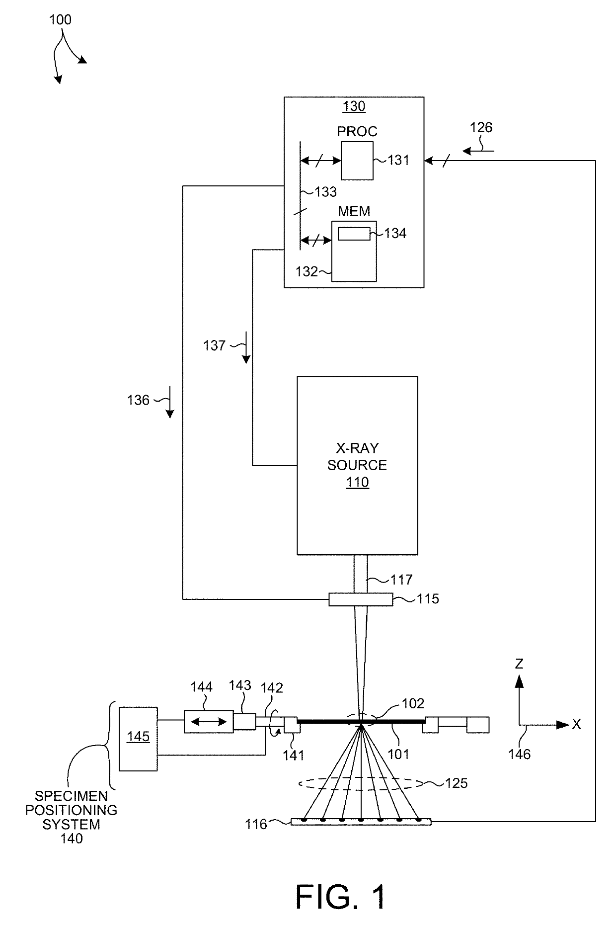
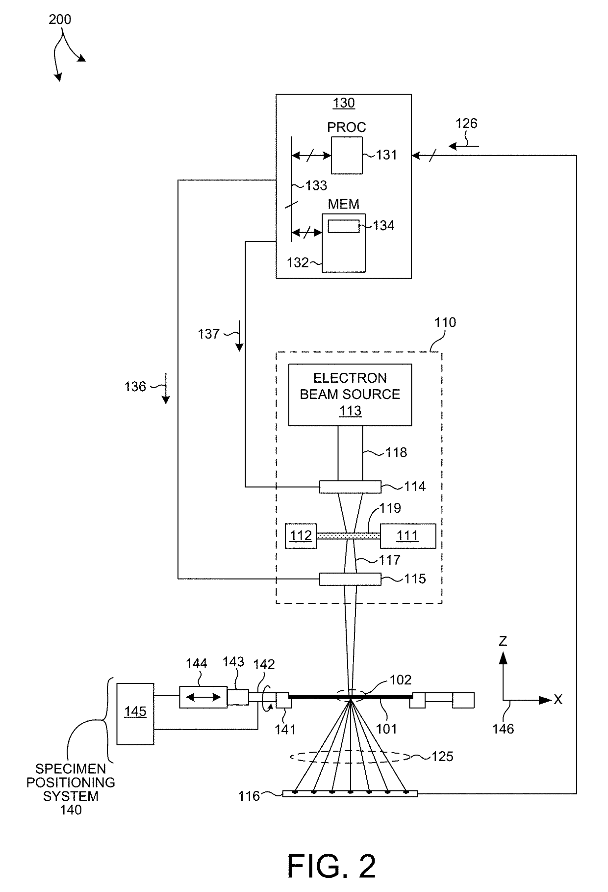
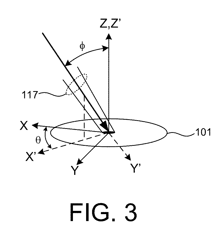
[0045]Methods and systems for improved measurement recipe generation to characterize dimensions and material properties of semiconductor structures are described herein. A metrology tool includes a wide array of measurement options. Measurement performance varies for each measurement option and measurement application. An improved measurement recipe identifies a minimum set of measurement options that increases wafer throughput while meeting measurement uncertainty requirements.

[0046]Metrology systems and techniques are employed to measure structural and material characteristics associated with different semiconductor fabrication processes. In some examples, optimized measurement recipes are employed for x-ray scatterometry measurements of critical dimensions, thicknesses, overlay, and material properties of high aspe...


PUM

PropertyMeasurementUnit
sizeaaaaaaaaaa
sizeaaaaaaaaaa
sizeaaaaaaaaaa

Abstract

Methods and systems for improving a measurement recipe describing a sequence of measurements employed to characterize semiconductor structures are described herein. A measurement recipe is repeatedly updated before a queue of measurements defined by the previous measurement recipe is fully executed. In some examples, an improved measurement recipe identifies a minimum set of measurement options that increases wafer throughput while meeting measurement uncertainty requirements. In some examples, measurement recipe optimization is controlled to trade off measurement robustness and measurement time. This enables flexibility in the case of outliers and process excursions. In some examples, measurement recipe optimization is controlled to minimize any combination of measurement uncertainty, measurement time, move time, and target dose. In some examples, a measurement recipe is updated while measurement data is being collected. In some examples, a measurement recipe is updated at a site while data is collected at another site.

Description

CROSS REFERENCE TO RELATED APPLICATION[0001]The present application for patent claims priority under 35 U.S.C. § 119 from U.S. provisional patent application Ser. No. 62 / 645,721, filed Mar. 20, 2018, the subject matter of which is incorporated herein by reference in its entirety. The present application for patent is related to U.S. patent application Ser. No. 15 / 419,130, filed Jan. 30, 2017, the subject matter of which is incorporated herein by reference in its entirety.TECHNICAL FIELD[0002]The described embodiments relate to metrology systems and methods, and more particularly to methods and systems for improved measurement accuracy.BACKGROUND INFORMATION[0003]Semiconductor devices such as logic and memory devices are typically fabricated by a sequence of processing steps applied to a specimen. The various features and multiple structural levels of the semiconductor devices are formed by these processing steps. For example, lithography among others is one semiconductor fabrication...

Claims


Application Information

Patent Timeline
Patent Type & Authority Applications(United States)
IPC IPC(8): G01N23/2055G03F7/20
CPCG01N23/2055G01N2223/1016G03F7/70616G01N2223/6116G03F7/70625H01L21/67242H01L22/30H01L22/20H01L22/10H01L21/027G03F7/70483G01N23/201G03F7/7065G01N2223/054G01N2223/303G01N2223/304G01N2223/305G01N2223/306G01N2223/645
Inventor GELLINEAU, ANTONIO ARION
Owner KLA CORP
Why Eureka
Try Eureka