
Hv converter with reduced EMI

a converter and emi technology, applied in the field of high voltage converters, can solve the problems of high emi noise and inability to optimize the pcb layout b>500/b>, and achieve the effect of minimizing electromagnetic interference (emi) noise and facilitating cooling

Active Publication Date: 2019-10-03
ALPHA & OMEGA SEMICON CAYMAN
View PDF5 Cites 4 Cited by
  • Summary
  • Abstract
  • Description
  • Claims
  • Application Information

AI Technical Summary

Benefits of technology

The present invention is about high voltage converters that use double-diffused metal-oxide semiconductor (DMOS) packages. These packages include a lead frame, a main DMOS chip, metal bumps, a connector, and molding encapsulation. The lead frame has a gate section, a source section, and a drain section. The main DMOS chip has a gate electrode and a source electrode on its bottom surface and a drain electrode on its top surface. The patent describes aPCB layout for a flyback converter that minimizes electromagnetic interference noise and cooling issues. The technical effects of this invention are the improved performance and reliability of high voltage converters.

Problems solved by technology

The performance of the PCB layout 500 is not optimized due to necessary tradeoff between thermal dissipation and EMI noise reduction.
However for high voltage applications such as 500V or higher, the EMI noise is high due to the fast changing and high drain voltage.
Furthermore, for high voltage applications, the high voltage drain lead with large area will demand large safety space therefore increasing the device area, making it challenge to minimize the device size while keeping safety space for high voltage.

Method used


Image

  • Hv converter with reduced EMI
  • Hv converter with reduced EMI
  • Hv converter with reduced EMI

Examples


Embodiment Construction

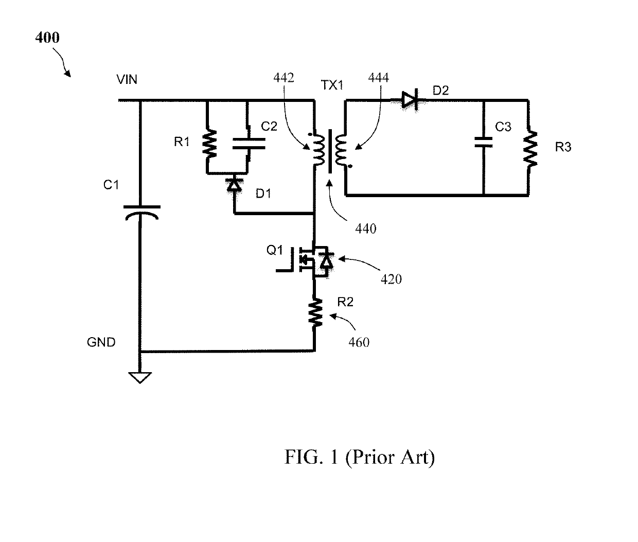
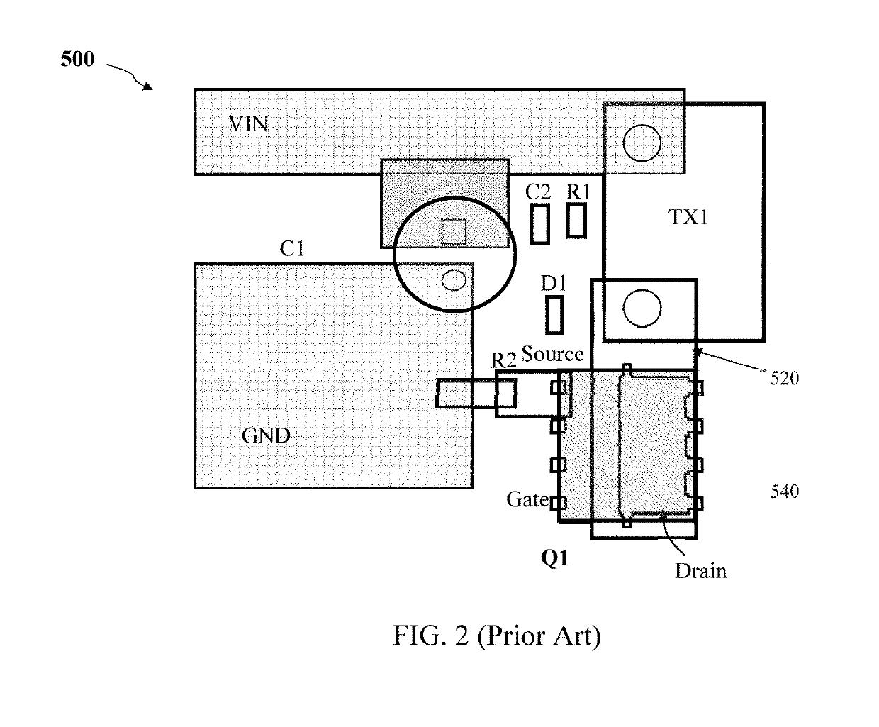
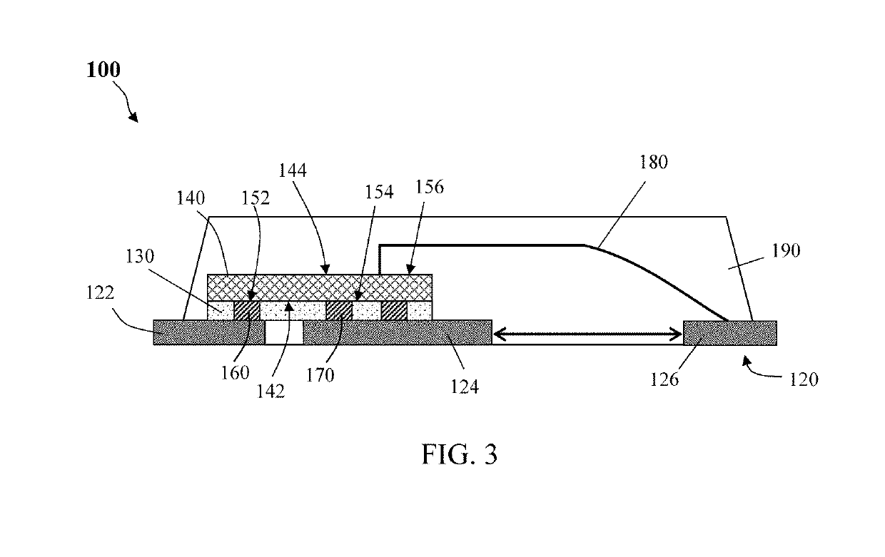
[0018]FIG. 3 is a cross sectional view of a double-diffused metal-oxide semiconductor (DMOS) package 100 in examples of the present disclosure. The DMOS package 100 includes a lead frame 120, an insulation material 130, a main DMOS chip 140, a first plurality of metal bumps 160, a second plurality of metal bumps 170, a wire 180 and a molding encapsulation 190. The lead frame 120 includes a gate section 122, a source section 124 and a drain section 126. To achieve thermal performance and to reduce EMI noise, in one example, the source section 124 accounts for more than 50% of the bottom surface area of the DMOS package 100. In another example, the source section 124 accounts for more than 70% of the bottom surface area of the DMOS package 100. In still another example, the source section 124 is 10 times in size of the drain section 126. The main DMOS chip 140 has a gate electrode 152 and a source electrode 154 disposed on a first surface 142 of the main DMOS chip 140 and a drain elec...


PUM


Abstract

A high voltage (HV) converter implemented on a printed circuit board (PCB) includes a double diffused metal oxide semiconductor (DMOS) package comprising a lead frame and a main DMOS chip. The lead frame includes a gate section electrically connected to a gate electrode of the main DMOS chip, a source section electrically connected to a source electrode of the main DMOS chip and a drain section electrically connected to a drain electrode of the main DMOS chip. The PCB layout includes a large area source copper pad attached to and overlapping the source section of the DMOS package to facilitate cooling and a small area drain copper pad attached to and overlapping the drain section of the DMOS package to reduce electromagnetic interference (EMI) noise.

Description

INCORPORATION BY REFERENCE[0001]The disclosure made in the U.S. Pat. No. 5,402,329 to Wittenbreder Jr. and U.S. Patent Application Publication Number 2017 / 0264206 to Rana et al. are hereby incorporated by reference.FIELD OF THE INVENTION[0002]This invention relates generally to high voltage converters using double-diffused metal-oxide semiconductor (DMOS) devices. More particularly, the present invention relates to a high voltage converter with improved electromagnetic interference (EMI) noise using an improved DMOS package.BACKGROUND OF THE INVENTION[0003]FIG. 1 shows circuitry 400 of a single-switch flyback converter in examples of the present disclosure. The single-switch flyback converter includes a switch 420, a transformer 440 and a resistor 460. The transformer 440 has a primary winding 442 and a secondary winding 444. A first end of the switch 420 is connected to a first end of the primary winding 442 of the transformer 440. A second end of the switch 420 is connected to the...

Claims


Application Information

Patent Timeline
Patent Type & Authority Applications(United States)
IPC IPC(8): H01L23/552H01L23/31H01L23/495H02M1/44H05K1/11H05K1/09H05K1/18
CPCH01L23/3114H01L23/4952H02M3/33569H01L23/49575H02M1/44H05K1/09H05K1/18H05K2201/10378H01L23/552H01L23/49562H05K2201/10022H02M3/33576H01L23/49568H05K1/111H05K2201/1003H01L23/49558H01L23/49503H01L29/7801H01L29/41725H01L23/49524H02M3/33592H01L23/3107H01L2224/48247H01L24/16H01L24/13H01L2224/131H01L2224/16245H01L24/73H01L24/32H01L24/29H01L2224/2919H01L2224/29191H01L2224/32245H01L2224/73204H01L2224/73265H01L2224/73257H01L24/48H01L2224/48096H01L2224/83385H01L2224/40247H01L2224/73255H01L2224/73263H01L2224/17107H01L2224/16258H01L2224/49176H01L2924/3025H01L2924/181H01L24/17H01L24/40H01L2224/40091H01L24/49H01L2924/19105Y02B70/10H01L2924/00014H02M1/342H02M3/01H01L2924/07025H01L2924/00H01L2224/84H01L2924/00012H01L2224/73221
Inventor NIU, ZHIQIANGCHANG, KUANG MINGCHEN, LINSUN, NINGHUANG, QIHONGLU, TZU-HSIN
Owner ALPHA & OMEGA SEMICON CAYMAN
Learn More