Printed circuit board device for an image capture module for a camera, image capture module that includes a printed circuit board device, and method for manufacturing a printed circuit board device

a printed circuit board and camera technology, applied in the direction of printed circuit non-printed electric components association, radiation controlled devices, printed circuit stress/warp reduction, etc., can solve the problems of local weakening of printed circuit boards, image sharpness may no longer be sufficient for image representation or image processing algorithms, etc., to achieve quick and efficient

Inactive Publication Date: 2020-02-13
ROBERT BOSCH GMBH
View PDF0 Cites 1 Cited by
  • Summary
  • Abstract
  • Description
  • Claims
  • Application Information

AI Technical Summary

Benefits of technology

[0023]The approach presented here also provides a device that is designed for carrying out, controlling, or implementing the steps of the method presented here in appropriate equipment. The object underlying the approach may also be quickly and efficiently achieved by this embodiment variant of the approach in the form of a device.

Problems solved by technology

As the result of thermal expansion and / or absorption of moisture by one or multiple elements of the image capture module, the printed circuit board may warp, thus changing a distance between the lens and the image sensor, so that in turn, an image sharpness may no longer be sufficient for an image representation or an image processing algorithm.
Such a through opening may locally weaken the printed circuit board.

Method used


Image

  • Printed circuit board device for an image capture module for a camera, image capture module that includes a printed circuit board device, and method for manufacturing a printed circuit board device
  • Printed circuit board device for an image capture module for a camera, image capture module that includes a printed circuit board device, and method for manufacturing a printed circuit board device
  • Printed circuit board device for an image capture module for a camera, image capture module that includes a printed circuit board device, and method for manufacturing a printed circuit board device

Examples


Embodiment Construction

[0036]In the following description of advantageous exemplary embodiments of the present approach, identical or similar reference numerals are used for the elements having a similar action which are illustrated in the various figures, and a repeated description of these elements is dispensed with.

[0037]If an exemplary embodiment includes an “and / or” linkage between a first feature and a second feature, this is to be understood in such a way that according to one specific embodiment, the exemplary embodiment has the first feature as well as the second feature, and according to another specific embodiment, the exemplary embodiment either has only the first feature or only the second feature.

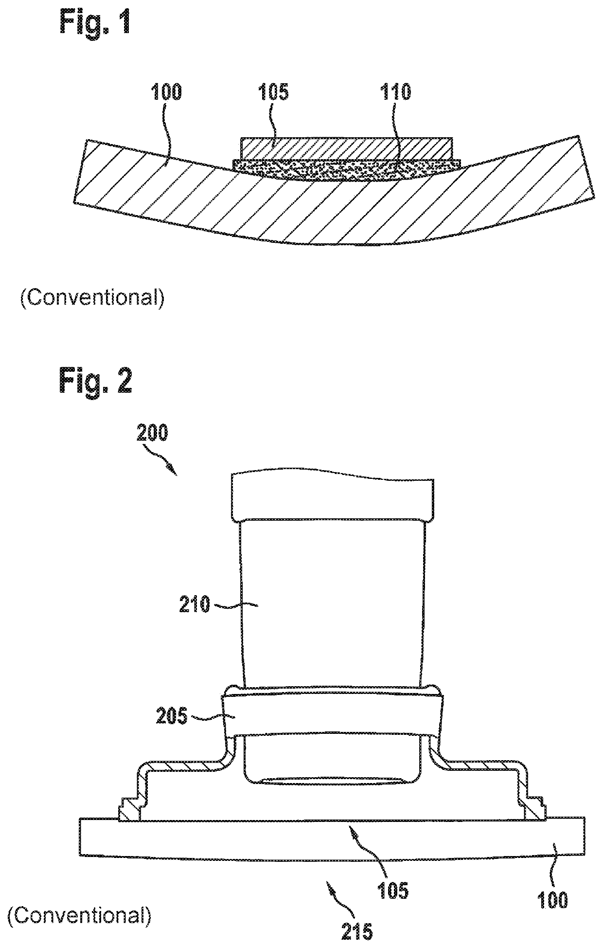
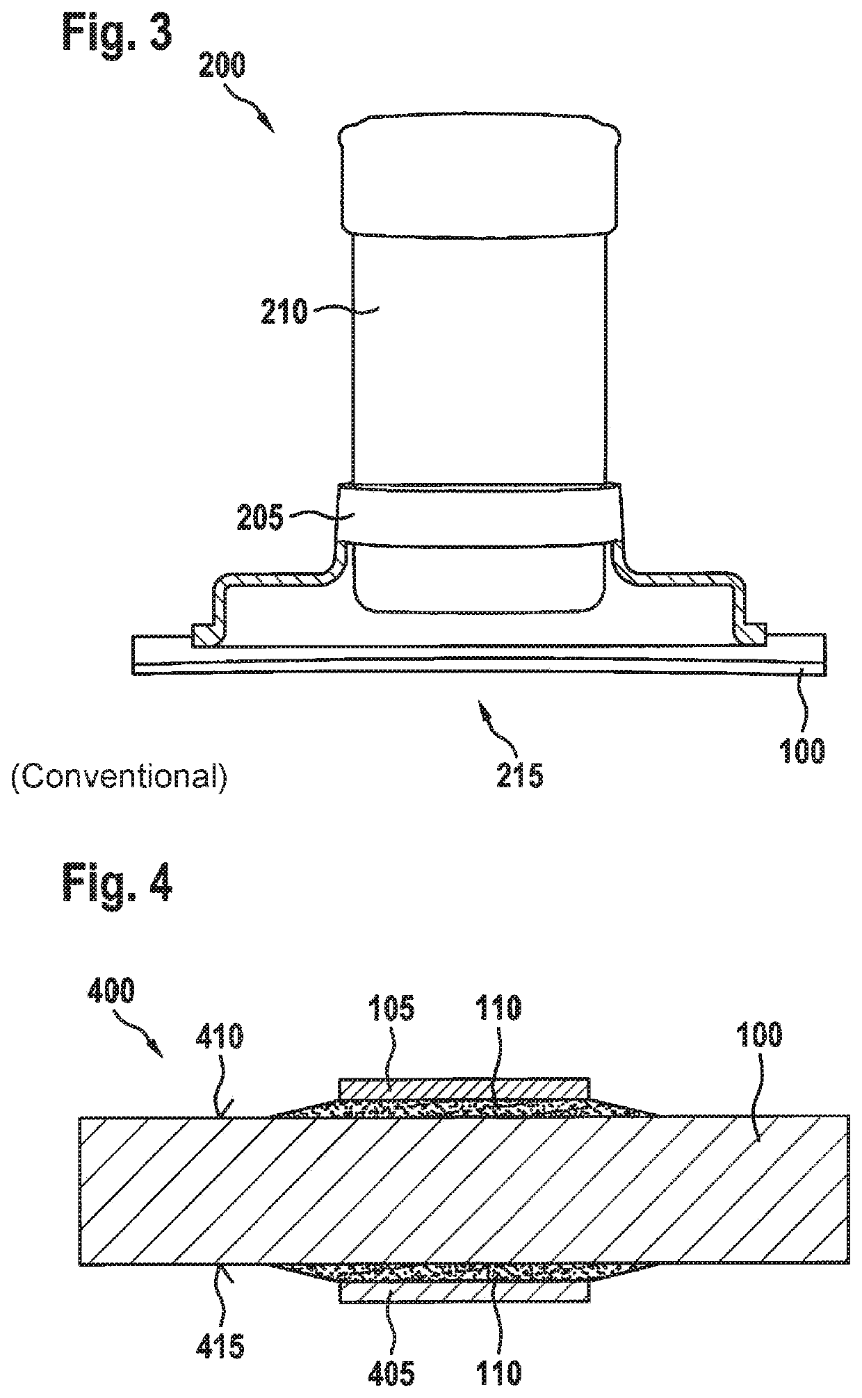
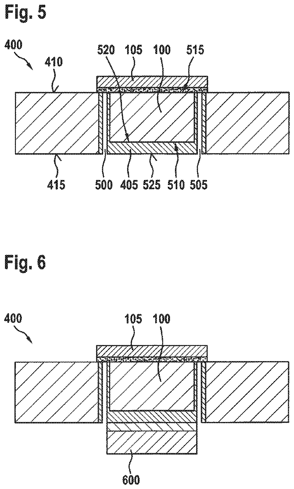
[0038]FIG. 1 shows a schematic cross-sectional illustration of a printed circuit board 100 with an image sensor 105. FIGS. 1 through 3 are used to illustrate a problem that is solved by the printed circuit board device presented in FIGS. 4 through 16.

[0039]FIG. 1 shows a conventional printed circuit...


PUM


Abstract

A printed circuit board device for an image capture module for a camera. The printed circuit board device includes a printed circuit board, an image sensor, and at least one copper layer and/or carbon layer. The printed circuit board includes a first main surface and a second main surface opposite from the first main surface. The image sensor is or may be situated on the first main surface of the printed circuit board. The copper layer that contains copper at least in part, and/or the carbon layer that contains carbon at least in part, are/is situated on the second main surface and formed for stabilization of the printed circuit board.

Description

CROSS REFERENCE[0001]The present application claims the benefit under 35 U.S.C. § 119 of German Patent Application No. DE 102018213146.5 filed on Aug. 7, 2018, which is expressly incorporated herein by reference in its entirety.FIELD[0002]The present invention is directed to a printed circuit board device, a method, and a computer program for manufacturing the printed circuit board device.BACKGROUND INFORMATION[0003]A common material for a flexible printed circuit board is a printed circuit board on a stainless steel substrate or a so-called FR4 printed circuit board made from a flame-retardant composite composed of epoxy resin and glass fiber fabric.[0004]Korean Patent KR 19980060521 U describes a printed circuit board with boreholes for protection from bending in some areas.SUMMARY[0005]The present invention provides a printed circuit board device for an image capture module for a camera, an image capture module that includes a printed circuit board device, and a method for manufa...

Claims


Application Information

Patent Timeline
Patent Type & Authority Applications(United States)
IPC IPC(8): H05K1/02H01L27/146H05K1/03H05K3/24
CPCH01L27/14601H05K1/0346H05K1/0271H05K3/24H05K1/0306H05K1/18H05K2201/10121H04N23/54H04N23/55H01L27/14618H05K2201/068H05K2201/09063H05K2201/0323H05K2201/09036H05K1/183
Inventor ESCHLER, JOHANNESWINKLER, MARTIN
Owner ROBERT BOSCH GMBH
Why Eureka
Try Eureka