GaN DRIVER USING ACTIVE PRE-DRIVER WITH FEEDBACK
- Summary
- Abstract
- Description
- Claims
- Application Information
AI Technical Summary
Benefits of technology
Problems solved by technology
Method used
Image
Examples
first embodiment
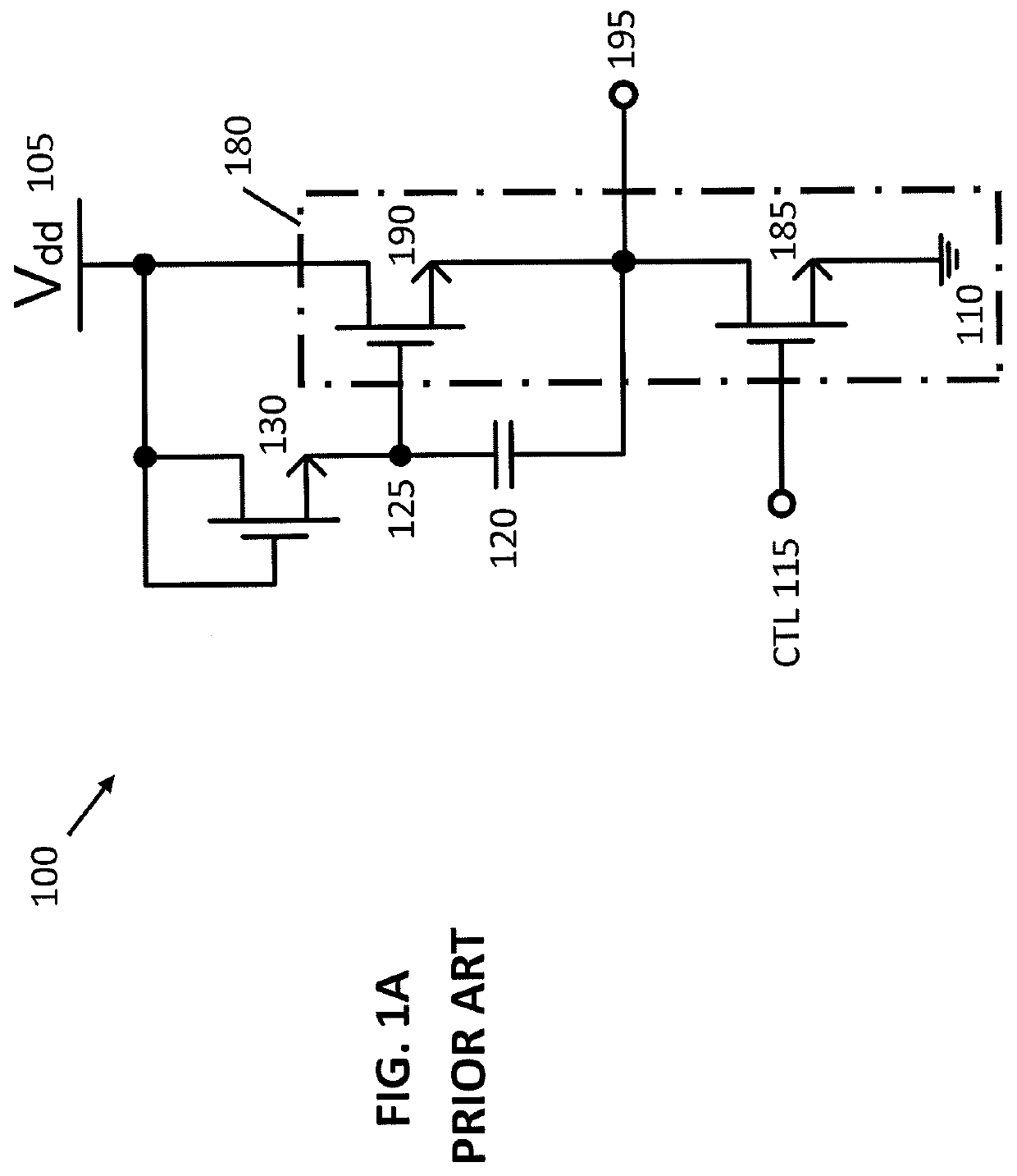
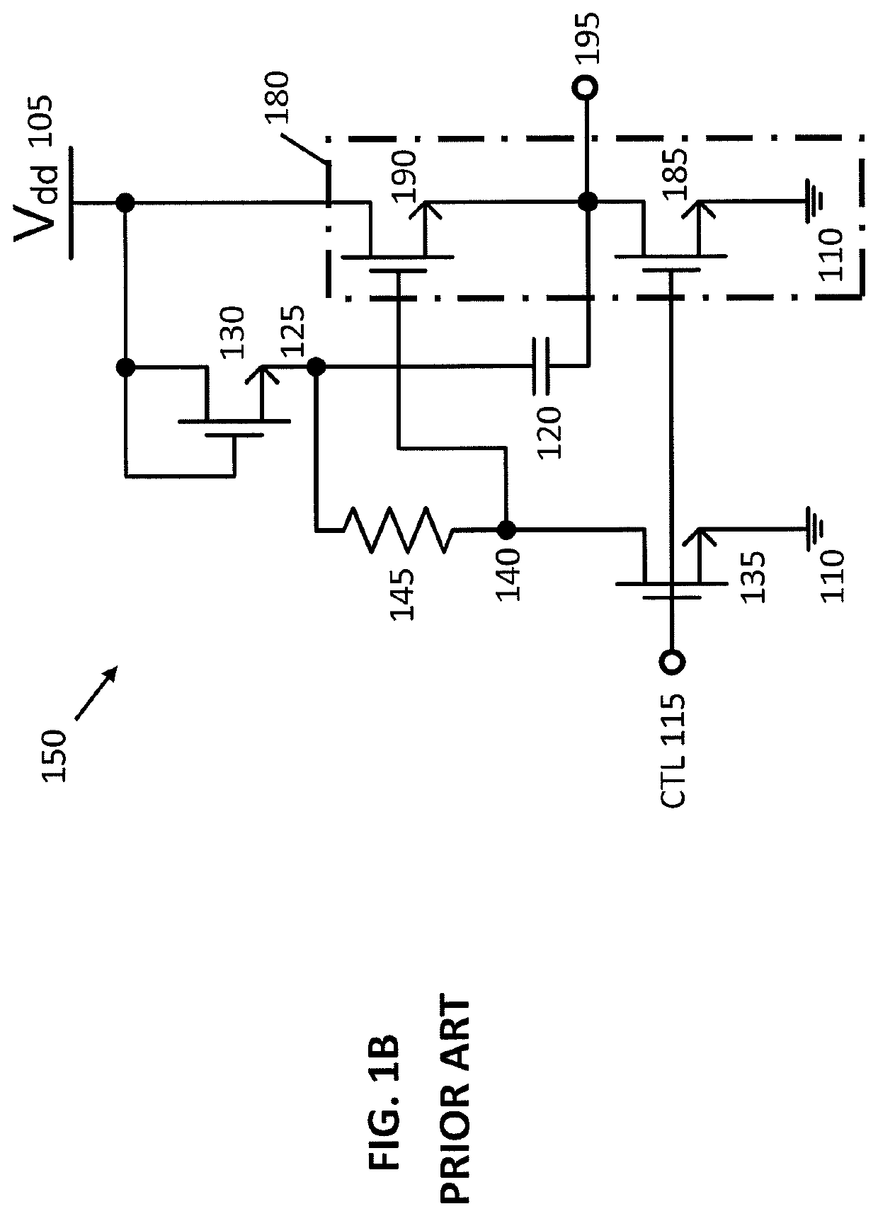
[0025]FIG. 3 illustrates a gate driver with an active pre-driver according to the present invention. Gate driver 300 includes an active pre-driver circuit 320 and an output stage 380, which comprises transistors 385 and 390, similar to output stage 180 and transistors 185 and 190 shown in FIGS. 1A-B. Active pre-driver circuit 320 includes transistors 325, 345, and 355, and resistor 335. Transistors 345 and 355 comprise the output stage 340 for active pre-driver circuit 320, similar to output stage 380 for gate driver 300. Transistors 390, 385, 325, 345, and 355 are preferably enhancement mode GaN FET semiconductor devices, which are monolithically integrated with the other components of gate driver 300 onto a single semiconductor die. Because GaN FETs are able to carry large currents, support high voltages, and switch more quickly than conventional transistors, gate driver 300 is able to increase and decrease the voltage on output node 395 more quickly than a similar system implemen...
second embodiment
[0032]FIG. 5 illustrates a gate driver with an active pre-driver having closed loop feedback according to the present invention. The active pre-driver of gate driver circuit 500 is similar to active pre-driver 320 shown in FIG. 3, but includes a feedback circuit 570 connected to nodes 530 and 550. Feedback circuit 570 is configured to keep the voltage on node 550 within a predetermined range of voltages centered around the desired voltage for node 550. In response to the voltage on node 550 exceeding above the predetermined range, feedback circuit 570 generates a feedback current IF 575, causing a voltage drop across resistor 535 and reducing the gate voltage of transistor 555. As a result, the voltage on the source terminal of transistor 555, i.e. the voltage at node 550 and output node 595, is decreased to be within the predetermined range. Feedback circuit 570 enables gate driver 500 to operate on a single, higher supply voltage by maintaining a lower, desired voltage on output n...
third embodiment
[0038]FIG. 7 illustrates a gate driver circuit 700 with an active pre-driver with closed loop feedback and an output stage, according to the present invention. Gate driver 700 includes an active pre-driver circuit 720 and an output stage 780, which comprises transistors 785 and 790, similar to output stage 180 and transistors 185 and 190 shown in FIG. 1A. Output stage 780 is connected to supply voltage source 705, which provides a higher supply voltage VddH. Active pre-driver circuit 720 includes transistors 725, 745, and 755, resistors 735 and 760, and feedback circuit 650 shown in FIG. 6B. Transistors 745 and 755 comprise an output stage 740 for active pre-driver circuit 720, similar to output stage 780 for gate driver 700.
[0039]In active pre-driver circuit 720, resistor 760 is chosen to have a resistance such that the voltage drop across resistor 760 is less than VTh in response to CTL 715 being logic high, keeping transistor 750 turned off. In some embodiments, resistor 760 is o...
PUM
 Abstract
Description
Claims
Application Information


