

Imaging element, stacked imaging element, and solid-state imaging apparatus
- Summary
- Abstract
- Description
- Claims
- Application Information
AI Technical Summary
Benefits of technology
Problems solved by technology
Method used
Image

Examples
embodiment 1
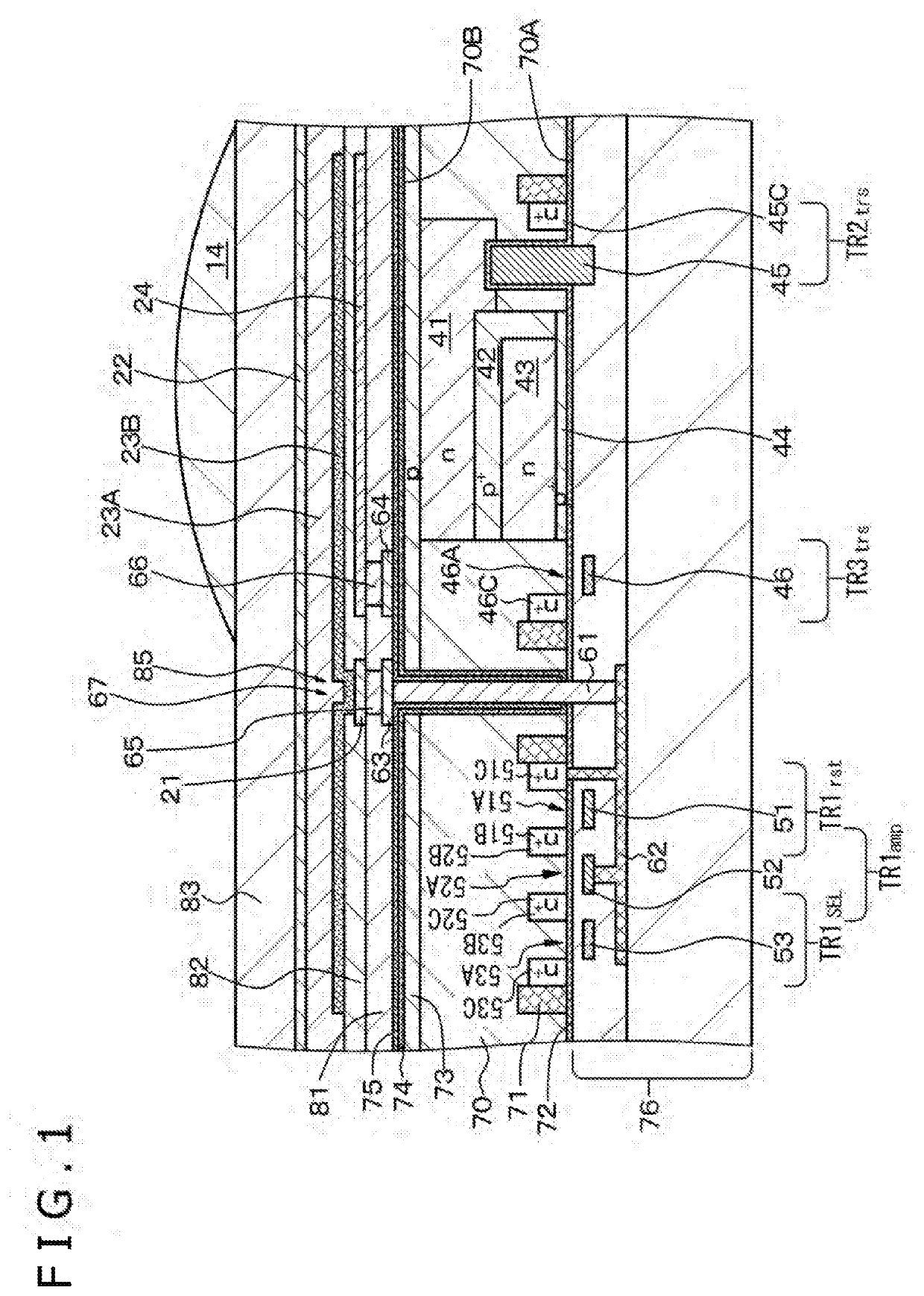
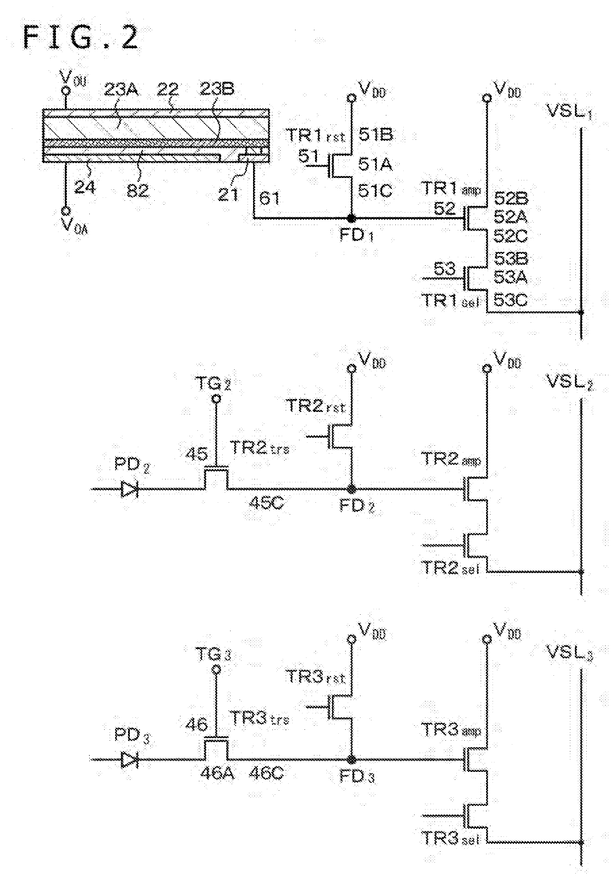
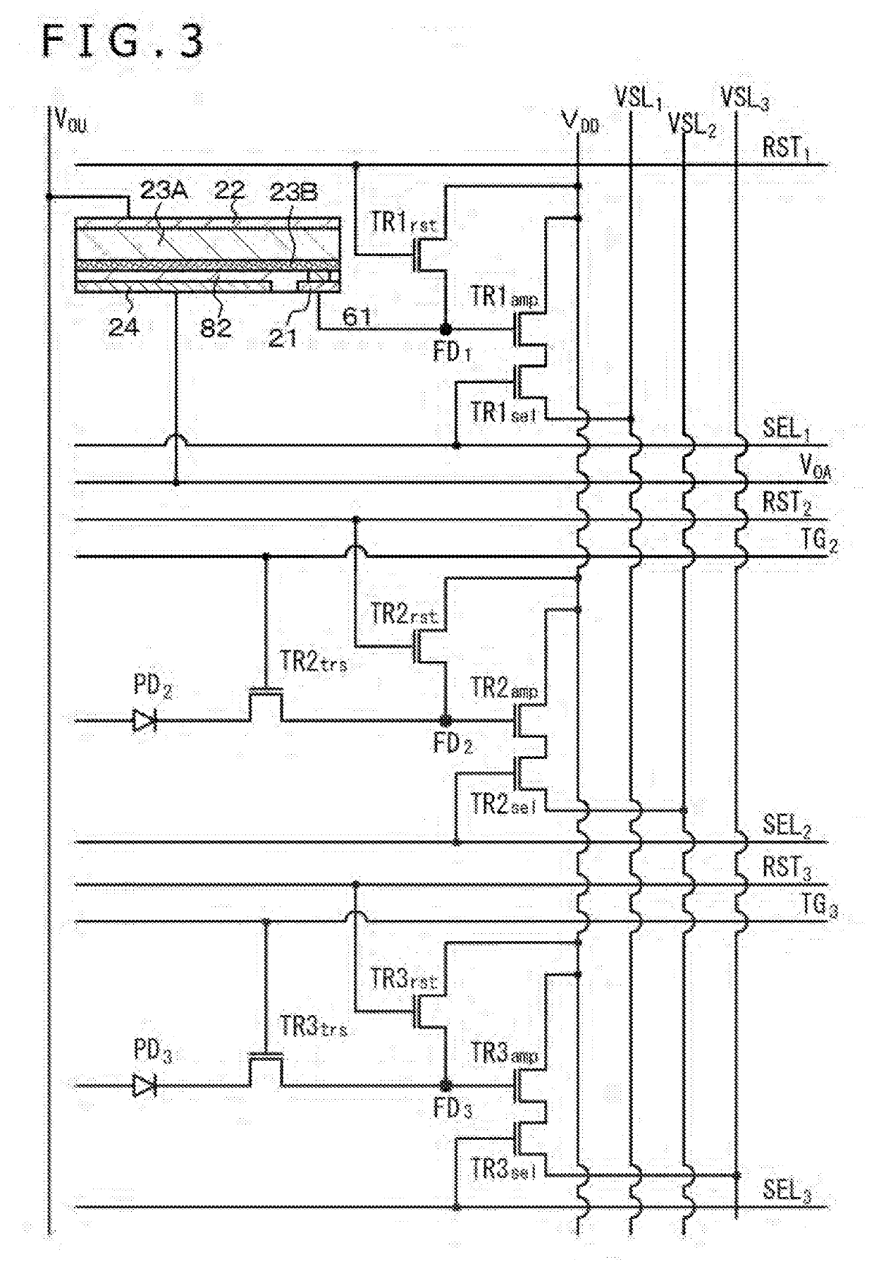
[0261]Embodiment 1 relates to the imaging elements according to the first to third aspects of the present disclosure, the stacked imaging element of the present disclosure, and the solid-state imaging apparatus according to the second aspect of the present disclosure. FIG. 1 illustrates a schematic partial cross-sectional view of the imaging element and the stacked imaging element (hereinafter, simply referred to as “imaging element”) of Embodiment 1. FIGS. 2 and 3 illustrate equivalent circuit diagrams of the imaging element of Embodiment 1. FIG. 4 illustrates a schematic layout drawing of a first electrode and a charge storage electrode included in a photoelectric conversion unit and transistors of a control unit included in the imaging element, of Embodiment 1. FIG. 5 schematically illustrates a state of potential in each section during operation of the imaging element of Embodiment 1. FIG. 6A illustrates an equivalent circuit diagram for describing each section of the imaging el...
embodiment 2
[0328]Embodiment 2 is a modification of Embodiment 1. An imaging element of Embodiment 2 illustrated in a schematic partial cross-sectional view of FIG. 11 is a front illuminated type imaging element. The imaging element has a stacked structure of three imaging elements including: a green light imaging element of first type in Embodiment 1 (first imaging element) sensitive to green the green light imaging element including a green light photoelectric conversion layer of first type for absorbing green light; a blue light imaging element in the past of second type (second imaging element) sensitive to blue light, the blue light imaging element including a blue light photoelectric conversion layer of second type for absorbing blue light; and a red light imaging element in the past of second type (third imaging element) sensitive to red light, the red light imaging element including a red light photoelectric conversion layer of second type for absorbing red light. Here, the red light im...
embodiment 3
[0332]Embodiment 3 is a modification of Embodiment 1 and Embodiment 2.
[0333]An imaging element of Embodiment 3 illustrated in a schematic partial cross-sectional view of FIG. 12 is a back illuminated type imaging element. The imaging element has a stacked structure of two imaging elements including the first imaging element of first type in Embodiment 1 and the second imaging element of second type. In addition, a modified example of the imaging element of Embodiment 3 illustrated in a schematic partial cross-sectional view of FIG. 13 provides a front illuminated type imaging element. The imaging element has a stacked structure of two imaging elements including the first imaging element of first type in Embodiment 1 and the second imaging element of second type. Here, the first imaging element absorbs light of primary colors, and the second imaging element absorbs light of complementary colors. Alternatively, the first imaging element absorbs white light, and the second imaging elem...
PUM
 Abstract
Description
Claims
Application Information