Gate Driver Circuitry for Power Transistors
a technology of power transistors and driver circuits, which is applied in the direction of pulse techniques, power conversion systems, amplifiers with semiconductor devices/discharge tubes, etc., can solve the problems of inacceptable components and assembly costs of external capacitors, and achieve accurate load regulation, reduce capacitance requirements, and fast response time
- Summary
- Abstract
- Description
- Claims
- Application Information
AI Technical Summary
Benefits of technology
Problems solved by technology
Method used
Image
Examples
first embodiment
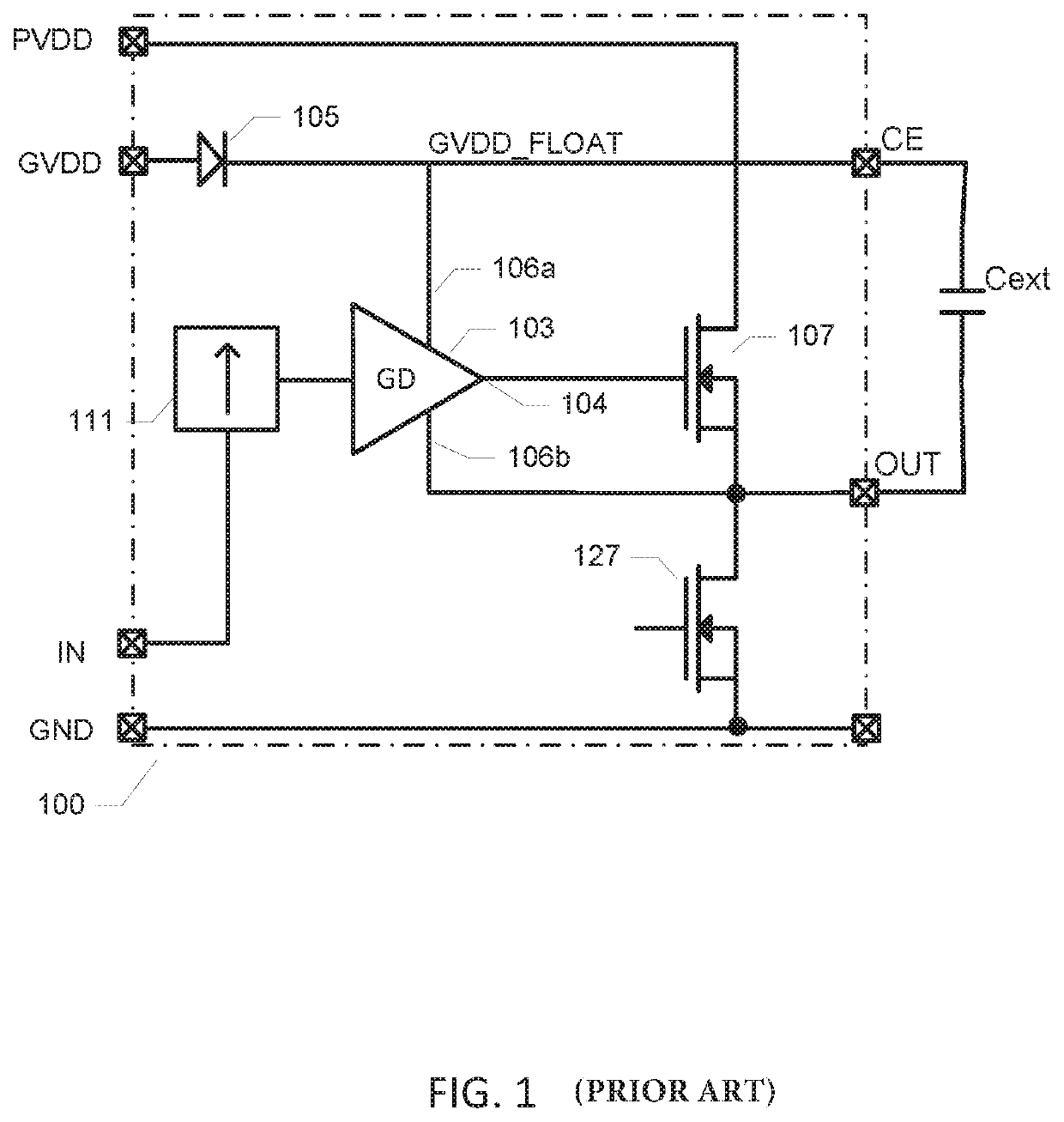
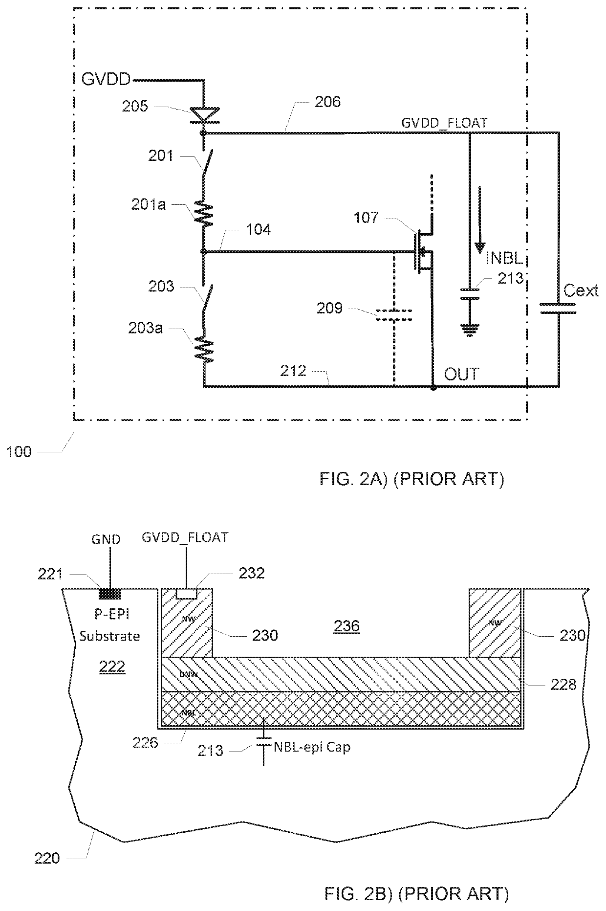
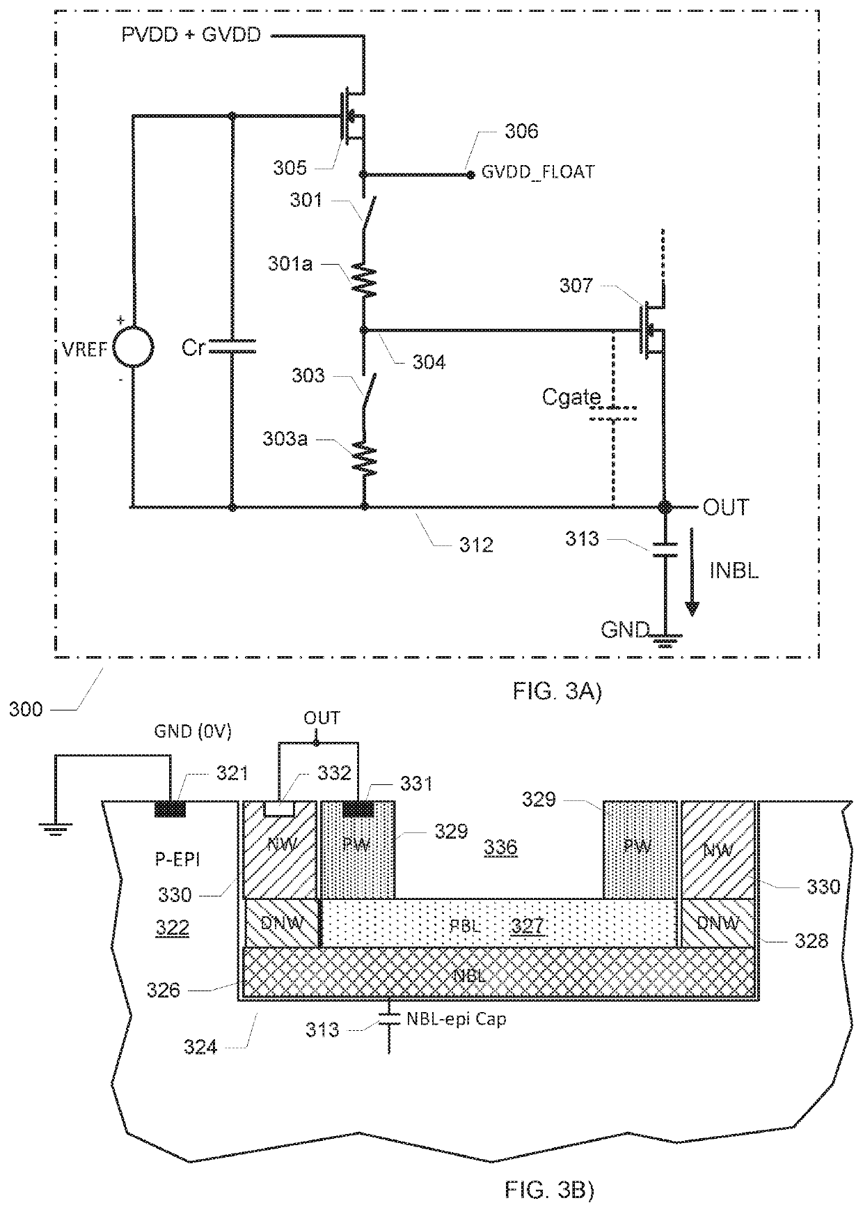
[0047]FIG. 3A) is a simplified schematic circuit diagram of a class D amplifier output stage 300 which comprises a regulated high side gate driver circuit in accordance with the invention. The skilled person will understand that the present regulated high side gate driver circuit in the alternative may be used to drive an output or power transistor of a single-phase or multiphase motor driver or a power transistor of a switched mode supply. The regulated high side gate driver structure is placed within the novel type of well-structure depicted on FIG. 3B) which shows a simplified cross-sectional view of the novel well structure 324. As illustrated on FIG. 3A), in the novel type of well-structure 324, the parasitic well capacitance 313 associated with the N-well diffusions 326, 330 is connected to the output terminal OUT of the class D amplifier output stage instead of to the high DC voltage terminal GVDD_FLOAT as was the case in the prior art gate driver circuit illustrated on FIG. ...
second embodiment
[0057]FIG. 5 shows a schematic circuit diagram of the regulated high side gate driver assembly or circuit 517. The present embodiment comprises an open loop topology floating voltage regulator 537 with a linear regulating device comprising a class AB output stage. Compared to the floating voltage regulator design discussed above, the present class AB output stage has the advantageous capability of both sourcing current out of, and sinking current into, the regulated DC voltage output GVDD_FLOAT. This feature may lead to a more effective suppression of high-frequency ac ripple and / or noise on the regulated DC voltage output GVDD_FLOAT 506.
[0058]The present regulated high side gate driver circuit 517 comprises the open-loop floating voltage regulator 537 coupled to a high side positive supply voltage port GVDD_FLOAT of an inverter configured gate driver 511. A high side negative supply voltage port 512 of the gate driver 511 is coupled to a negative regulator input of the floating vol...
PUM
 Abstract
Description
Claims
Application Information


