ESD protection in an electronic device

a technology of electronic devices and protection, applied in semiconductor devices, semiconductor/solid-state device details, electrical apparatus, etc., can solve the problems of significantly reducing esd robustness, and achieve the effect of increasing the resistance of a parasitic path and increasing the resistance of the parasitic path

Active Publication Date: 2020-04-30
INFINEON TECH AG
View PDF0 Cites 2 Cited by
  • Summary
  • Abstract
  • Description
  • Claims
  • Application Information

AI Technical Summary

Benefits of technology

[0189]In processing operation 1150, the fabricator resource 140 implements silicide blocking on a periphery region of the first transistor circuit. Absence of the silicide material over the periphery region of the first transistor circuit provides increased resistance of a parasitic path formed via a combination of the first transistor circuit and the second transistor circuit.
[0...

Problems solved by technology

Triggering of the parasitic transistors can reduce ESD robustness significantly either by degradin...

Method used


Image

  • ESD protection in an electronic device
  • ESD protection in an electronic device
  • ESD protection in an electronic device

Examples


Embodiment Construction

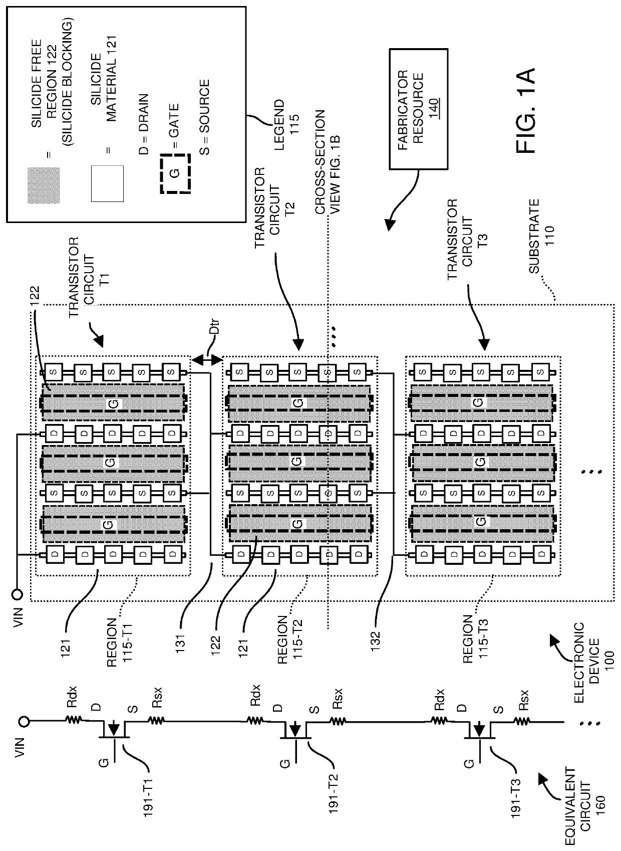
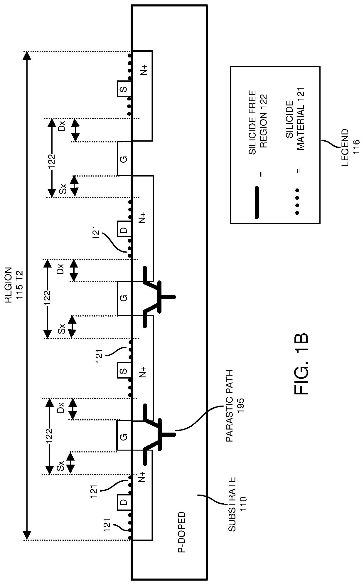
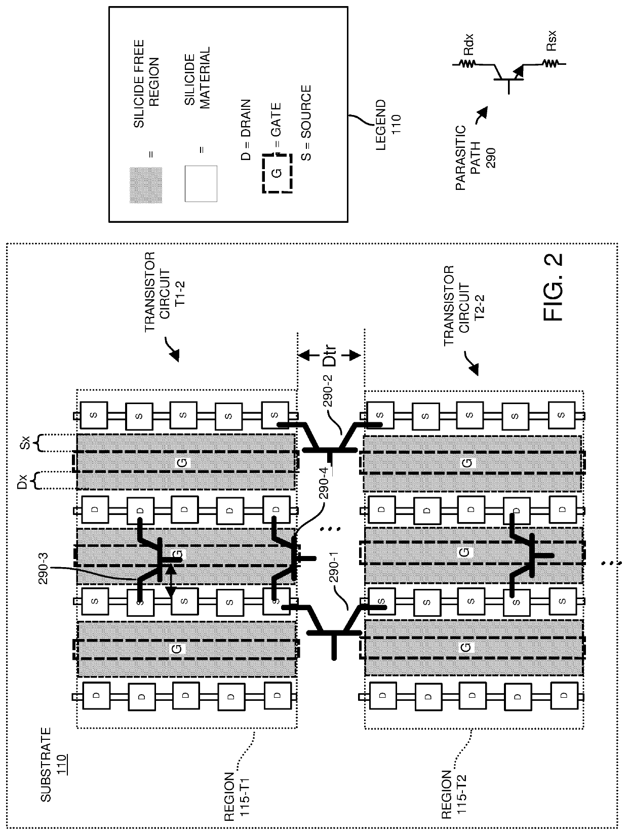
[0062]According to one configuration, a fabricator produces an electronic device to include: a substrate; a transistor circuit disposed on the substrate; silicide material disposed on first regions of the transistor circuit. Via silicide blocking, the fabricator prevents the silicide material from being present over second regions of the transistor circuit. Absence of the silicide material over the second regions of the respective transistor circuit increases a resistance of one or more parasitic paths (such as one or more parasitic transistors) in the electronic device. The increased resistance in the one or more parasitic paths, such as due to strategic placement of silicide material and / or preventing silicide material from being disposed or present on certain surface portions of the electronic device, provides better protection of the electronic device and corresponding transistor circuits against electro-static discharge conditions.

[0063]Now, more specifically, FIG. 1A is an exa...


PUM


Abstract

According to one configuration, a fabricator produces an electronic device to include: a substrate; a transistor circuit disposed on the substrate; silicide material disposed on first regions of the transistor circuit; and the silicide material absent from second regions of the transistor circuit. Absence of the silicide material over the second regions of the respective of the transistor circuit increases a resistance of one or more parasitic paths (such as one or more parasitic transistors) in the transistor circuit. The increased resistance in the one or more parasitic paths provides better protection of the transistor circuit against electro-static discharge conditions.

Description

RELATED APPLICATIONS[0001]This application is related to and claims the benefit of earlier filed U.S. Provisional Patent Application Ser. No. 62 / 753,412 entitled “ESD PROTECTION IN AN ELECTRONIC DEVICE,” (Attorney Docket No. 2018P51752US), filed on Oct. 31, 2018, the entire teachings of which are incorporated herein by this reference.BACKGROUND[0002]Conventional RF-stacks (which means a number of RF-transistors connected in series) comprising fully-silicided NMOS (N-type Metal Oxide Semiconductor) transistors in series (such N=2 to 32 transistors or more) can be applied in a CMOS (Complementary MOS) bulk process technology on an extremely high-resistive substrate (low doped substrate) with a volume resistivity in the range of ρ_bulk=100 to 10 k Ohm centimeter. The MOS bulk corresponds to the substrate.[0003]During normal RF (Radio Frequency) operating conditions of such a device, the low doped substrate is fully depleted by application of a negative substrate DC bias voltage.[0004]T...

Claims


Application Information

Patent Timeline
IPC IPC(8): H01L23/60H01L23/522H01L29/66H01L21/285
CPCH01L23/60H01L23/522H01L29/66575H01L21/28518H01L29/4238H01L29/41758H01L27/0266H01L27/0288
Inventor MERGENS, MARKUSSIMBUERGER, WERNER
Owner INFINEON TECH AG
Why Eureka
Try Eureka