Implementing logic function and generating analog signals using nor memory strings

a logic function and logic string technology, applied in the field of high-density memory structure, can solve the problems of long latency, limiting the number of transistors that can be programmed in parallel, and not being read or programmed

Active Publication Date: 2020-07-16
SUNRISE MEMORY CORP
View PDF0 Cites 98 Cited by
  • Summary
  • Abstract
  • Description
  • Claims
  • Application Information

AI Technical Summary

Benefits of technology

[0017]According to one embodiment of the present invention, a NOR memory string may be used to implement a logic function involving many Boolean variables, or to generate an analog signal whose magnitude is representative of the bit values of...

Problems solved by technology

Under this NAND arrangement, the activated TFTs that are not read or programmed may experience undesirable program-disturb or read-disturb conditions.
The low read current that is required to be conducted through a long NAND string results in a long latency.
Channel hot-electron injection programming requires a relatively large electron current t...

Method used


Image

  • Implementing logic function and generating analog signals using nor memory strings
  • Implementing logic function and generating analog signals using nor memory strings
  • Implementing logic function and generating analog signals using nor memory strings

Examples


Embodiment Construction

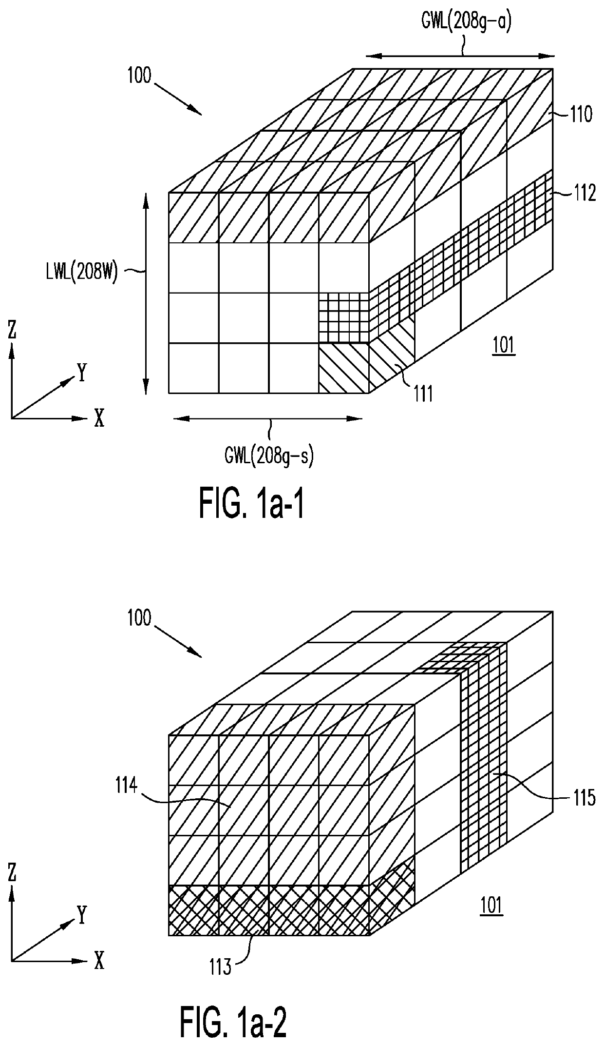
[0070]FIGS. 1a-1 and 1a-2 show conceptualized memory structure 100, illustrating in this detailed description an organization of memory cells according to embodiments of the present invention. As shown in FIG. 1a-1, memory structure 100 represents a 3-dimensional memory array or block of memory cells formed in deposited thin-films fabricated over a surface of substrate layer 101. Substrate layer 101 may be, for example, a conventional silicon wafer used for fabricating integrated circuits, familiar to those of ordinary skill in the art. In this detailed description, a Cartesian coordinate system (such as indicated in FIG. 1a-1) is adopted solely for the purpose of facilitating description. Under this coordinate system, the surface of substrate layer 101 is considered a plane which is parallel to the X-Y plane. Thus, as used in this description, the term “horizontal” refers to any direction parallel to the X-Y plane, while the term “vertical” refers to the Z-direction. As shown, bloc...


PUM


Abstract

NOR memory strings may be used for implementations of logic functions involving many Boolean variables, or to generate analog signals whose magnitudes are each representative of the bit values of many Boolean variables. The advantage of using NOR memory strings in these manners is that the logic function or analog signal generation may be accomplished within one simultaneous read operation on the NOR memory strings.

Description

CROSS REFERENCE TO RELATED APPLICATIONS[0001]The present invention is a continuation-in-part application of U.S. non-provisional patent application Ser. No. 16 / 582,996 (“Non-provisional Application I”), entitled “Memory Circuit, System and Method for Rapid Retrieval of Data Sets,” filed on Sep. 25, 2019, which is a continuation application of U.S. non-provisional patent application (“Non-Provisional Application II”), Ser. No. 16 / 107,306, entitled “System Controller and Method for Determining the Location of the Most Current Data File Stored on a Plurality of Memory Circuit,” filed on Aug. 21, 2018, which is a divisional application of U.S. non-provisional patent application (“Non-provisional Application III”), Ser. No. 15 / 248,420, entitled “Capacitive-Coupled Non-Volatile Thin-Film Transistor Strings in Three Dimensional Arrays,” filed on Aug. 26, 2016, which is related to and claims priority of (i) U.S. provisional application (“Provisional Application I”), Ser. No. 62 / 235,322, ent...

Claims


Application Information

Patent Timeline
IPC IPC(8): G11C16/34G11C16/04G11C11/56H01L29/10H01L29/08H01L29/786H01L29/92H01L27/11582G11C16/10H01L21/28H01L29/66H01L29/792
CPCH01L29/40117H01L29/0847H01L29/78633H01L27/11582G11C11/5635G11C16/10G11C11/5628G11C16/3431H01L29/92G11C16/0416G11C11/5642H01L29/7926G11C16/0491H01L29/1037G11C16/0483H01L29/66833H01L27/11565G11C16/0466H01L29/78642H10B41/10H10B43/10H10B41/27H10B43/27G06N3/063G11C16/26G06F17/16
Inventor SALAHUDDIN, SAYEEFNORMAL, ROBERT D.HARARI, ELI
Owner SUNRISE MEMORY CORP
Why Eureka
Try Eureka