Method of topology-selective film formation of silicon oxide

Active Publication Date: 2020-08-06
ASM IP HLDG BV
View PDF0 Cites 165 Cited by
  • Summary
  • Abstract
  • Description
  • Claims
  • Application Information

AI Technical Summary

Problems solved by technology

On the other hand, in a certain semiconductor device-manufacturing process, there is demand for non-uniform formation of film, e.g., in gate spacers wherein only sidewall portions of film deposited in trenches are selectively left in certain areas, and in that case, film deposition by ALD is used in combination with anisotropic dry etching to form a desired pattern.
However, because it is difficult to determine the end point of

Method used


Image

  • Method of topology-selective film formation of silicon oxide
  • Method of topology-selective film formation of silicon oxide
  • Method of topology-selective film formation of silicon oxide

Examples


example 1

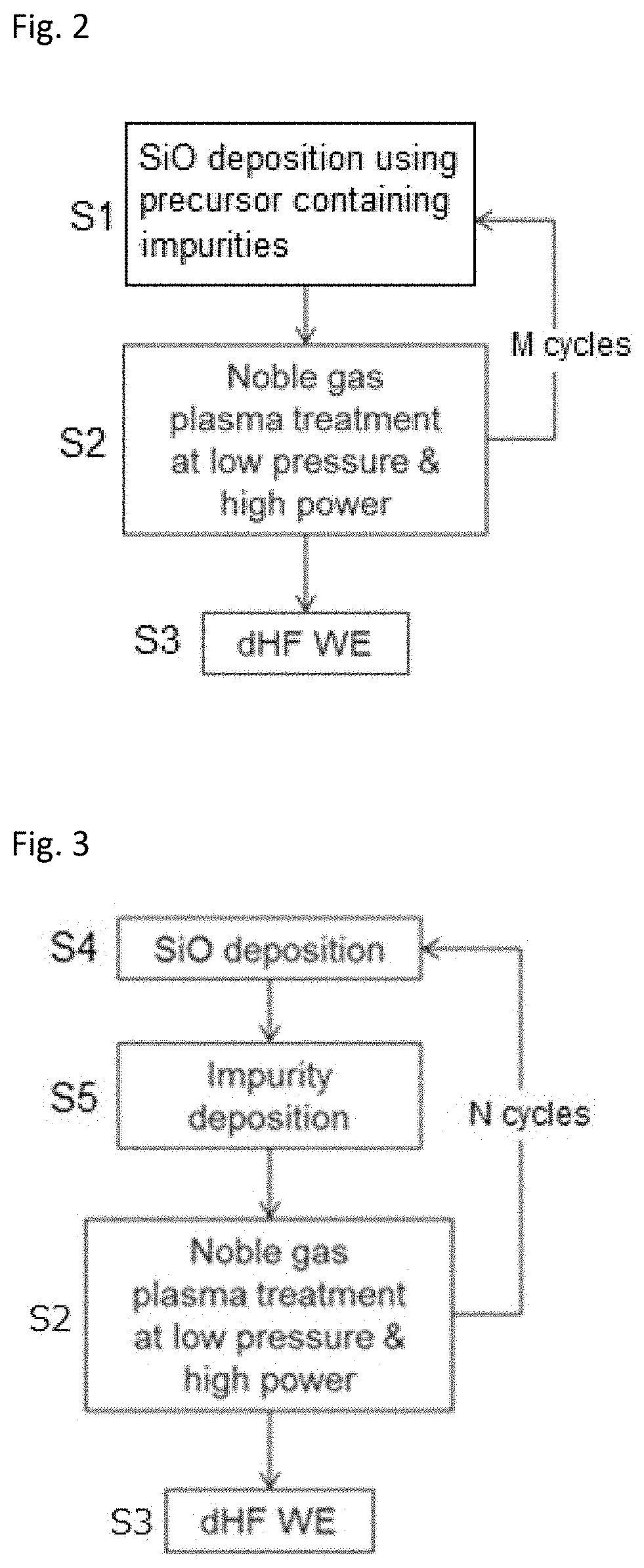
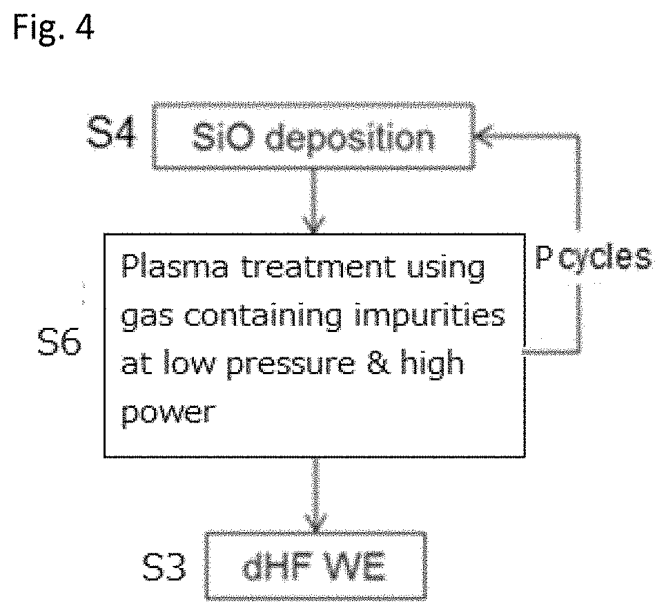
[0065]In this example, the sidewall-thick TS—SiO by area-selective incorporation of impurities was conducted as illustrated in FIG. 4. However, this example was rather an experimental example, since step S6 in FIG. 4 was conducted using polyimide tape (with an acryl adhesive) with which a substrate adhered to a susceptor, which tape was exposed to a plasma and expected to be a source of impurities including carbon (airborne-molecular contaminants, AMC) which was released into the plasma, forming a plasma containing active species of carbon (as opposed to forming a plasma containing active species of impurities by adding a gas containing impurities to a plasma gas). The above step is considered to be functionally equivalent to step S6, wherein both steps produce a plasma containing active species of impurities.

[0066]First, a SiO film was formed on a Si substrate (Φ300 mm) having trenches by PEALD, one cycle of which was conducted under the conditions shown in Table 5 (deposition cycl...

reference example 1

[0072]In this reference example, consistent with the above in Example 1, it was confirmed that impurities (carbon and nitrogen) were incorporated into a film by plasma treatment at a low pressure, and a portion of the film containing more impurities was more vulnerable to wet etching.

[0073]A film (blanket film) was deposited in a manner substantially similar to that in Example 1, and then, the film was exposed to a plasma in a manner substantially similar to that in Example 1 except that the treatment pressure was changed as shown in FIG. 7, followed by wet etching in a manner substantially similar to that in Example 1. FIG. 7 is a graph showing the relationship between treatment pressure [kPa] and wet etch rate (“WERR. Tox”: wet etch rate relative to thermal oxide) of the films. As shown in FIG. 7, when the treatment pressure was 100 Pa (“No. 2”), WERR was very high (i.e., low quality film with low resistance to chemicals), whereas when the treatment pressure was 500 Pa, 2,000 Pa, ...

##ic example 1

Prophetic Example 1

[0076]In this example, the sidewall-thick TS—SiO by area-selective incorporation of impurities is performed as illustrated in FIG. 3. A SiO film is deposited in a manner substantially similar to that in Example 1 as step S4 in FIG. 3. In place of use of polyimide tape with an acryl adhesive in Example 1, upon deposition of the film, without breaking a vacuum, CxHy gas (x and y are integers other than zero) and Ar are introduced to the chamber at about 0.5 slm and about 2 slm, respectively, so as to expose the film to the hydrocarbon gas for about one minute, thereby adsorbing impurities (e.g., carbon) onto a surface of the film. Thereafter, step S2 in FIG. 3 is conducted under conditions similar to those for the plasma treatment in Example 1, followed by wet etching (step S3 in FIG. 3) under the conditions similar to those in Example 1. As a result, the sidewall-thick TS—SiO having a topology similar to that shown in (c) in FIG. 6 is achieved.


PUM

PropertyMeasurementUnit
Fractionaaaaaaaaaa
Pressureaaaaaaaaaa
Dielectric polarization enthalpyaaaaaaaaaa

Abstract

A method for forming a dielectric film containing a Si—O bond a trench formed in an upper surface of a substrate, includes: designing a topology of a final dielectric film containing a Si—O bond formed in the trench by preselecting a target portion to be selectively removed relative to a non-target portion of an initial dielectric film resulting in the final dielectric film; conformally depositing the initial dielectric film on the upper surface and in the trench; and relatively increasing an amount of impurities contained in the target portion of the initial dielectric film relative to an amount of impurities contained in the non-target portion of the initial dielectric film to obtain a treated dielectric film, thereby giving the target portion and the non-target portion different chemical resistance properties when subjected to etching.

Description

CROSS-REFERENCE TO RELATED APPLICATIONS[0001]This application claims the benefit of U.S. Provisional Patent Application No. 62 / 800,210 filed on Feb. 1, 2019, the disclosure of which is incorporated herein in its entirety by reference.BACKGROUNDField of the Invention[0002]The present invention relates generally to a method for forming a dielectric film containing a Si—O bond on a step formed on a surface of a substrate, particularly, a method of topology-selective film formation of silicon oxide.Related Art[0003]Atomic layer deposition (ALD) is characterized not only by excellent controllability over film thickness and excellent uniformity of film, but also by being capable of depositing a film uniformly covering a three-dimensional structure, and accordingly, ALD has been recognized to be a very important deposition method in the semiconductor industry. On the other hand, in a certain semiconductor device-manufacturing process, there is demand for non-uniform formation of film, e.g....

Claims


Application Information

Patent Timeline
IPC IPC(8): H01L21/02H01L21/311
CPCH01L21/0228H01L21/02208H01L21/02164H01L21/31111H01L21/02321H01L21/02225H01L21/02263H01L21/0337H01L21/02274H01L21/02211H01L21/02126H01L21/311C23C16/401C23C16/56C23C16/45536C23C16/505C23C16/45553C09K13/08H01L21/306
Inventor ZAITSU, MASARUFUKAZAWA, ATSUKI
Owner ASM IP HLDG BV
Why Eureka
Try Eureka