Image sensor

Active Publication Date: 2020-08-20
HUA WEI SEMICONDUCTOR (SHANGAHAI) CO LTD
View PDF0 Cites 0 Cited by
  • Summary
  • Abstract
  • Description
  • Claims
  • Application Information

AI Technical Summary

Benefits of technology

The present invention provides an image sensor that can transmit high-resolution image data at a faster rate with fewer terminals for external electrical connection. This is achieved by using a peripheral circuit to drive the VCSEL and outputting a second optical pulse, which further reduces the number of terminals required and simplifies the design of the mating device. Overall, this results in a smaller and more efficient image sensor that can handle high-speed, high-bandwidth data transmission.

Problems solved by technology

Therefore, the electrical connection terminals are relatively bulky compared to the image sensor' package size, thus hindering the miniaturization of the image sensor.
Additionally, the number of the electrical connection terminals on the image sensor is relative large, and as the mating device is required to have the same number of electrical connection terminals, it is possible to undesirably increase the structural complexity of the mating device.
Further, this conventional image sensor usually communicates electrical signals, which tend to limit the transmission rate and experience attenuation and thus do not allow a large data transfer.

Method used


Image

  • Image sensor
  • Image sensor
  • Image sensor

Examples


Embodiment Construction

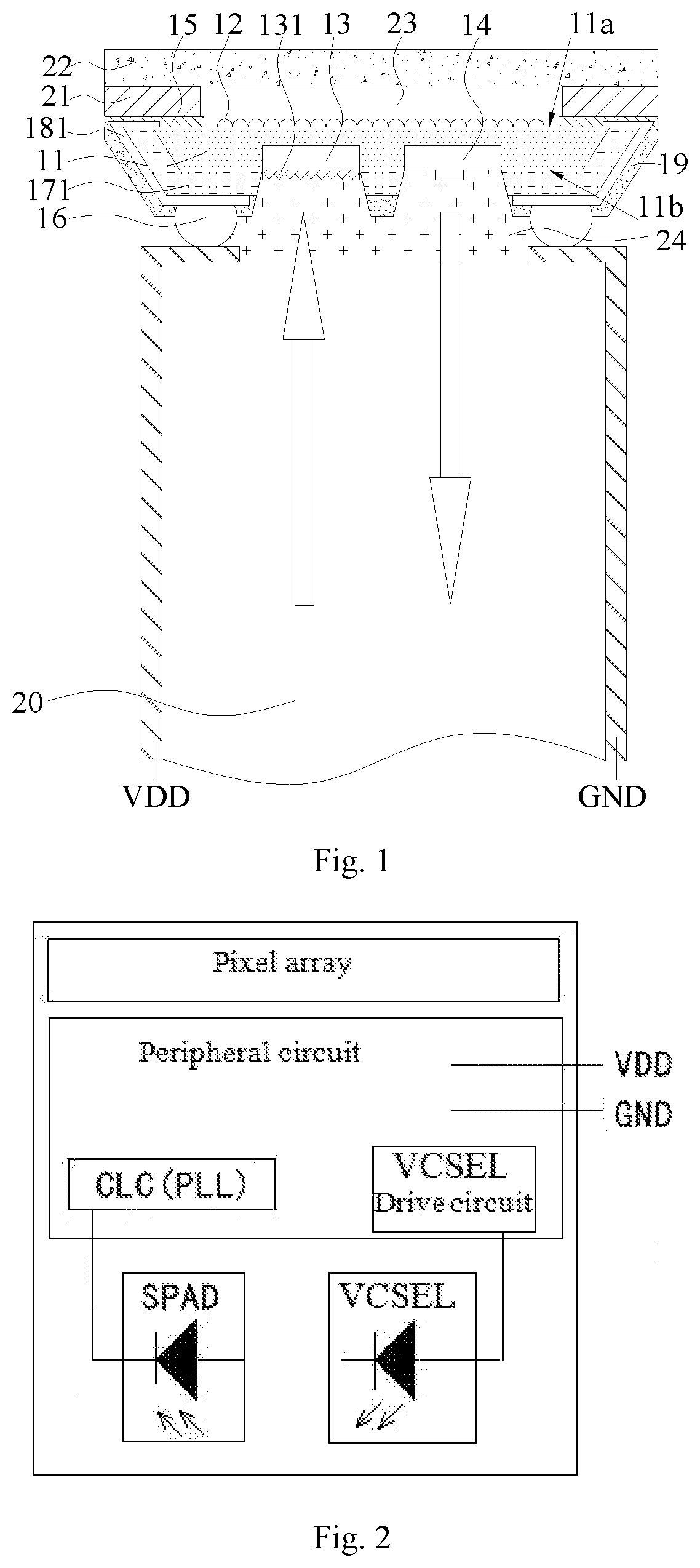
[0028]A few specific embodiments of the invention will be described in greater detail with reference to the accompanying drawings. Features and advantages of the invention will become more apparent from the following description. Note that the drawings are provided in a very simplified form not necessarily drawn to scale, and their only intention is to facilitate convenience and clarity in explaining the embodiments.

[0029]The present invention provides an image sensor. Referring to FIG. 1, the image sensor according to an embodiment of the present invention includes:

[0030]a substrate 11, a pixel array 12 integrated to the substrate 11, a peripheral circuit (not shown), a single-photon avalanche diode (SPAD) detector 13 and a vertical-cavity surface-emitting laser (VCSEL) 14.

[0031]The peripheral circuit is configured to process an electrical signal resulting from photoelectric conversion in the pixel array 12.

[0032]The SPAD detector 13 is configured to convert a first external optica...


PUM


Abstract

An image sensor is disclosed which includes a substrate, a pixel array, a peripheral circuit, an SPAD detector and a VCSEL integrated in the substrate. The peripheral circuit is configured to process an electrical signal obtained from photoelectric conversion in the pixel array, the SPAD detector is configured to convert a first external optical pulse into an electrical pulse to provide a clock signal to the peripheral circuit. The VCSEL is driven by the peripheral circuit and configured to output a second optical pulse. The number of electrical connection terminals in the image sensor is reduced to only two, which is favorable to the miniaturization of the image sensor and simplifies the design of the mating device while allowing the inputting of a first optical pulse and outputting of a second optical pulse. By using these optical signals, extremely high speed and high bandwidth data transmission can be achieved.

Description

CROSS-REFERENCE TO RELATED APPLICATION[0001]This application claims the priority of Chinese patent application number 201910113625.1, filed on Feb. 14, 2019, the entire contents of which are incorporated herein by reference.TECHNICAL FIELD[0002]The present invention relates to the field of integrated circuits (ICs) and, in particular, an image sensor.BACKGROUND[0003]In the field of minimally invasive surgery, image sensors have been widely used, for example, in electro-endoscopes. Since an electro-endoscope is used to allow direct observation of an internal cavity or an organ's lumen in the body, in which it is inserted, it is required to have small dimensions. Accordingly, it is necessary for image sensors in such applications to be very small, for example, having a package size of 1.8 mm×1.8 mm, 1 mm×1 mm or even smaller. For image sensors imposed with such harsh requirements on compactness, the number and distribution of terminals on the image sensors for external electrical conn...

Claims


Application Information

Patent Timeline
IPC IPC(8): H01L31/12H04N5/378H04N5/335H01L31/107H01L27/146H01L31/02H01L31/0216H01S5/026H01S5/022
CPCH04N5/3355H01L31/107H01L31/02005H01L27/14636H04N5/225H01L31/02162H01L27/14643H04N5/378H01L31/12H01S5/02284H04N5/2257H01S5/0262H04N2005/2255H01S5/18369H01L31/153A61B1/051G02B6/4212G02B6/4246H01S5/423H01S5/4087H01S5/0427H01S5/02345H04N23/555H04N23/54H04N23/57H04N25/709H04N25/79H01S5/02251H04N23/00H04N25/75H04N25/772
Inventor FAN, CHUN-SHENG
Owner HUA WEI SEMICONDUCTOR (SHANGAHAI) CO LTD
Why Eureka
Try Eureka