Supercharge Your Innovation With Domain-Expert AI Agents!

Bootstrap diode with low substrate leakage current

a technology of bootstrap diodes and substrates, applied in the direction of diodes, semiconductor devices, electrical apparatus, etc., can solve the problems of bootstrap diodes failing at their sole purpose of conducting unidirectionally, current leaking to the semiconductor substrate, and normal bootstrap diodes not being able to sustain high voltag

Inactive Publication Date: 2020-09-17
NUVOTON
View PDF0 Cites 0 Cited by
  • Summary
  • Abstract
  • Description
  • Claims
  • Application Information

AI Technical Summary

Benefits of technology

The invention aims to prevent a leakage current from flowing through a specific region of a semiconductor device. This is achieved by configuring three wells and a buried layer to lower the current flow. Overall, the invention aims to improve the stability and reliability of the semiconductor device.

Problems solved by technology

However, when the bootstrap diode is forward biased, there is a drawback in that there is current leaking to the semiconductor substrate.
In addition, a normal bootstrap diode cannot sustain high voltages.
When the bootstrap diode is reverse-biased by voltage that is too high, the bootstrap diode would break down and be turned ON, causing the bootstrap diode to fail at its sole purpose of conducting unidirectionally.

Method used


Image

  • Bootstrap diode with low substrate leakage current
  • Bootstrap diode with low substrate leakage current
  • Bootstrap diode with low substrate leakage current

Examples


Embodiment Construction

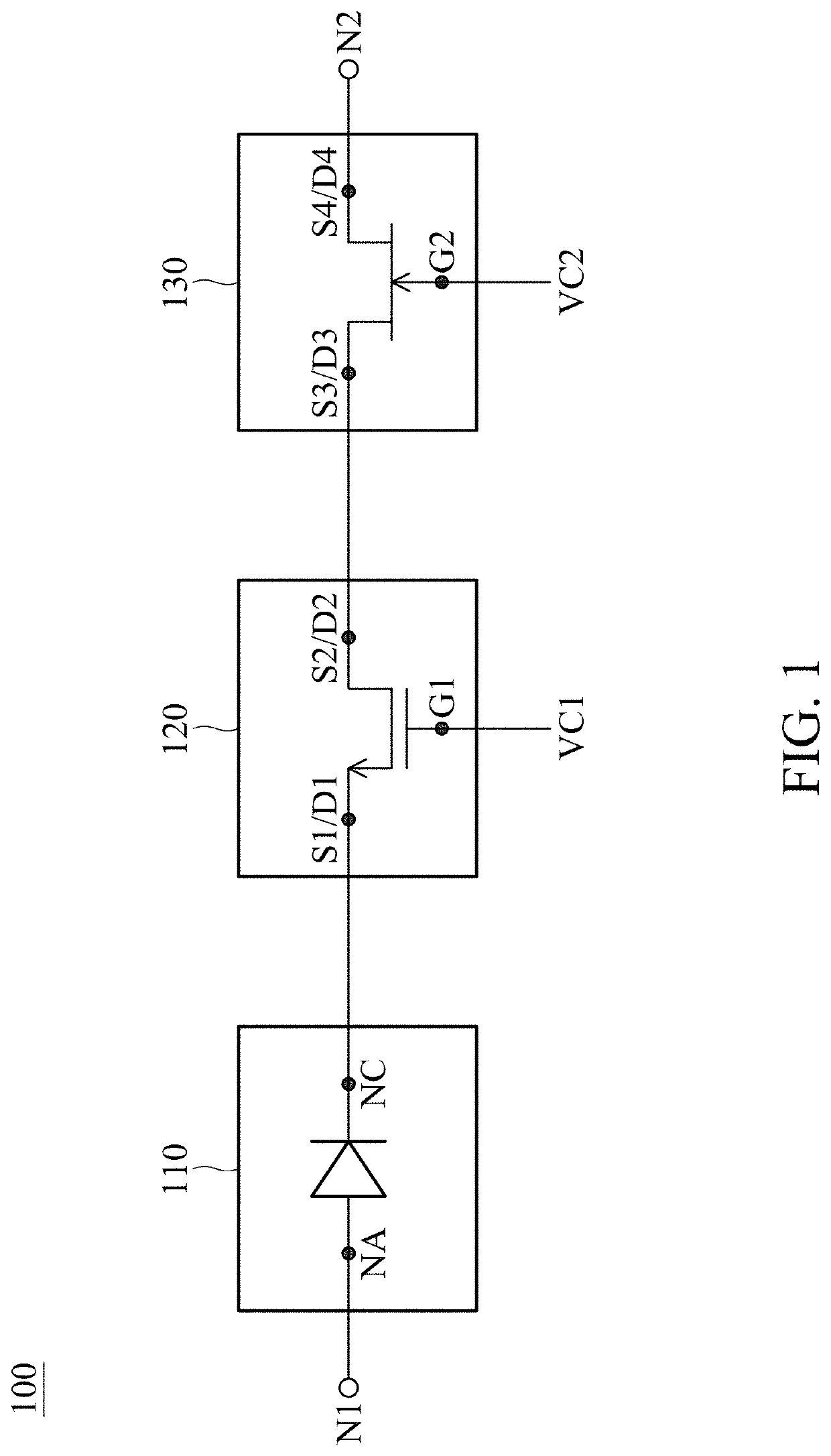
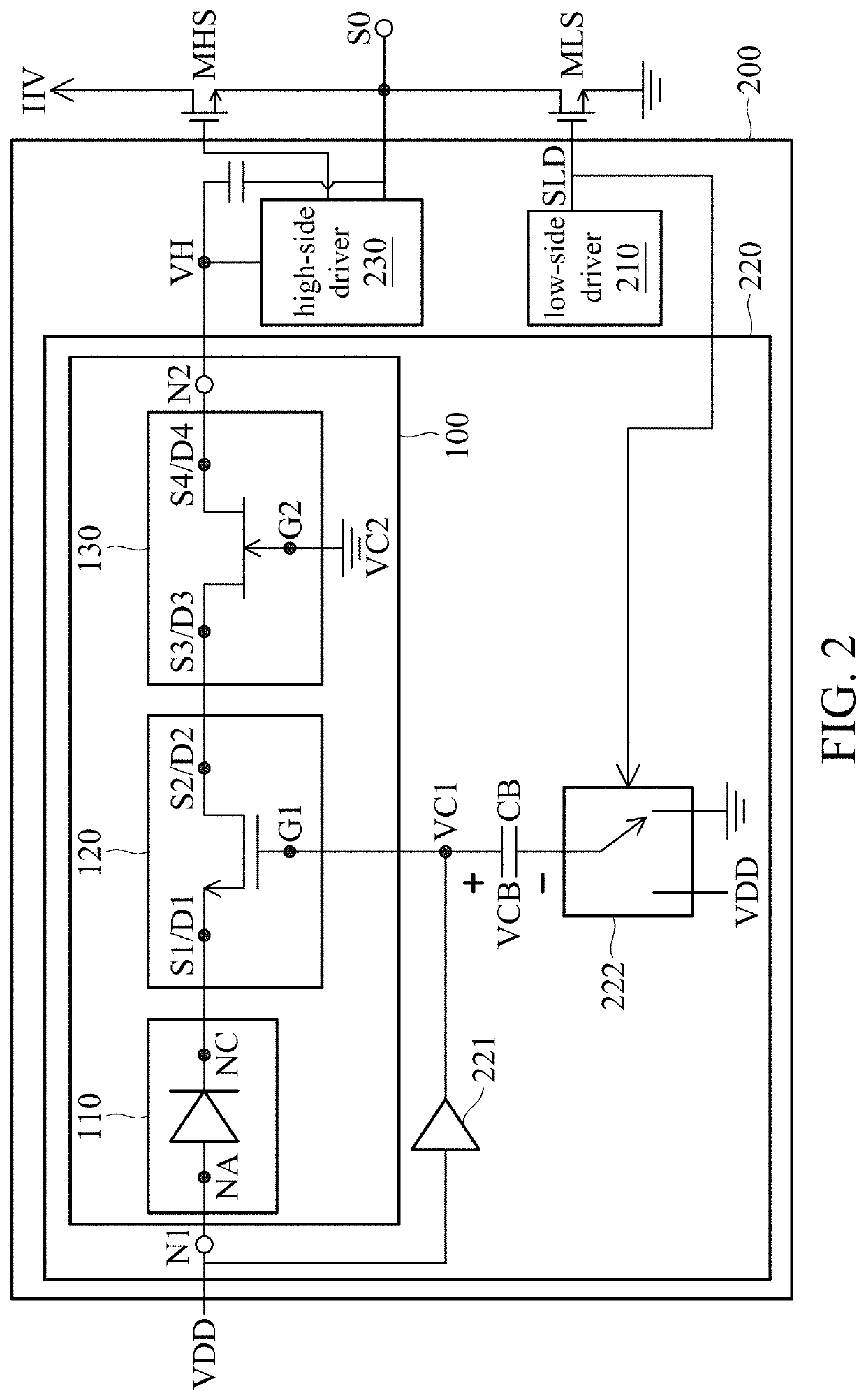
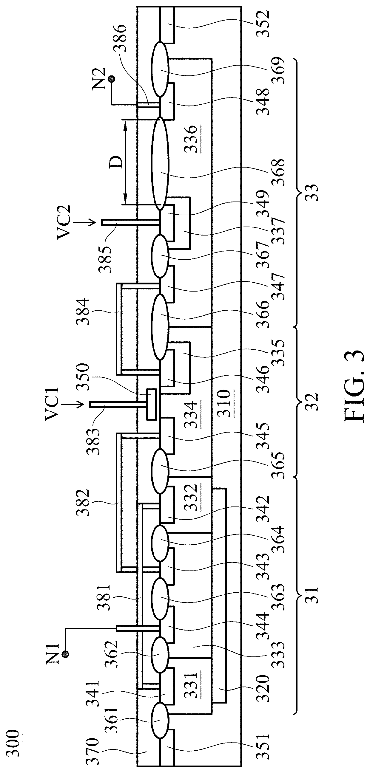
[0032]The semiconductor device of the present disclosure is described in detail in the following description. In the following detailed description, for purposes of explanation, numerous specific details and embodiments are set forth in order to provide a thorough understanding of the present disclosure. The specific elements and configurations described in the following detailed description are set forth in order to clearly describe the present disclosure. It will be apparent, however, that the exemplary embodiments set forth herein are used merely for the purpose of illustration, and the inventive concept may be embodied in various forms without being limited to those exemplary embodiments. In addition, the drawings of different embodiments may use like and / or corresponding numerals to denote like and / or corresponding elements in order to clearly describe the present disclosure. However, the use of like and / or corresponding numerals in the drawings of different embodiments does no...


PUM


Abstract

A semiconductor device includes a diode, a metal-oxide semiconductor, and a junction field-effect transistor. The diode includes an anode node and a cathode node, wherein the anode node is coupled to a first node. The metal-oxide semiconductor includes a first source / drain terminal, a second source / drain terminal, and a first gate terminal, wherein the first source / drain terminal is coupled to the cathode node and the first gate terminal receives a first control voltage. The junction field-effect transistor includes a third source / drain terminal, a fourth source / drain terminal, and a second gate terminal, wherein the second gate terminal receives a second control voltage, the third source / drain terminal is coupled to the second source / drain terminal, and the fourth source / drain terminal is coupled to a second node.

Description

CROSS REFERENCE TO RELATED APPLICATIONS[0001]This Application claims priority of Taiwan Patent Application No. 108108769, filed on Mar. 15, 2019, the entirety of which is incorporated by reference herein.BACKGROUND OF THE INVENTIONField of the Invention[0002]The disclosure relates generally to a semiconductor device, and more particularly it relates to a bootstrap diode having no substrate leakage current.Description of the Related Art[0003]Improving power efficiency has been a great concern. Off-line power converters that are capable of reducing power consumption are also becoming increasingly important. In response to changes in the consumer market, HVIC chips have gradually been adopted more widely because they have better performance and are capable of satisfying low-cost so a designer has the flexibility to achieve solutions when implementing high-performance power converters.[0004]An example of the effects of the HVIC chip is the gate driver, which is used to drive a metal-oxi...

Claims


Application Information

Patent Timeline
IPC IPC(8): H01L27/02
CPCH01L27/0274H01L27/0255H01L27/0203H01L29/0603H01L29/0684H01L29/861H01L27/0251H01L27/0266
Inventor NINGARAJU, VIVEKCHEN, PO-AN
Owner NUVOTON
Features
  • R&D
  • Intellectual Property
  • Life Sciences
  • Materials
  • Tech Scout
  • Unparalleled Data Quality
  • Higher Quality Content
  • 60% Fewer Hallucinations
Learn More