
Curable silicone composition and optical semiconductor device

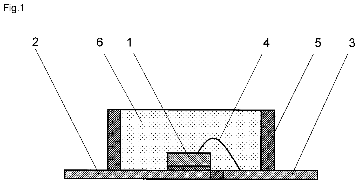
a silicone composition and silicone technology, applied in semiconductor devices, semiconductor/solid-state device details, coatings, etc., can solve the problems of contaminating the case, insufficient light extraction efficiency of the light emitting element, color unevenness or chromaticity deviation in the obtained optical semiconductor device, etc., to achieve minimal color unevenness or chromaticity deviation, good light extraction efficiency, and minimal contamination of the case

Inactive Publication Date: 2020-12-10
DOW TORAY CO LTD
View PDF0 Cites 0 Cited by
  • Summary
  • Abstract
  • Description
  • Claims
  • Application Information

AI Technical Summary

Benefits of technology

The present invention introduces a curable silicone composition that is ideal for producing optical semiconductor devices. These devices have minimal contamination, good light extraction, and minimal color unevenness or chromaticity deviation. The invention ensures that the case of the device is always clean during production. This composition is easy to apply and has good adhesion properties, which make it a great choice for creating optical semiconductor devices.

Problems solved by technology

However, blending a phosphor into a curable silicone composition is problematic in that the phosphor precipitates and separates during storage, or the phosphor precipitates and separates due to a drop in viscosity of the composition while the composition is heated and cured, resulting in insufficient efficiency of light extraction from the light emitting element or the occurrence of color unevenness or chromaticity deviation in the obtained optical semiconductor device.
Furthermore, because a curable silicone composition containing a phenyl group has low affinity with the case (frame material) of an optical semiconductor device, some optical semiconductor devices are also problematic in that part of the curable silicone composition crawls on the case surface and contaminates the case when the optical semiconductor device is produced.

Method used


Image

  • Curable silicone composition and optical semiconductor device
  • Curable silicone composition and optical semiconductor device
  • Curable silicone composition and optical semiconductor device

Examples


synthesis example 1

[0076]First, 102.52 g of an organopolysiloxane represented by the formula:

352.53 g of an allyloxy polyalkylene oxide represented by the formula:

CH2═CH—CH2—O—(CH2CH2O)4(CH2CH(CH3)O)18H,

150.0 g of isopropyl alcohol, and 0.1875 g of an isopropyl alcohol solution of a platinum-1,3-divinyl-1,1,3,3-tetramethyldisiloxane complex (platinum content=4 mass %) were charged into a four-neck flask equipped with a stirrer, a reflux condenser, and a thermometer and then heated at 80° C. for 2 hours. Next, 82.7 g of vinyl tris(trimethylsiloxy)silane was charged and heated for 2 hours. Further, 7.2 g of 1-hexene was charged and heated for 2 more hours. After the disappearance of silicon-hydrogen bonds in the reaction mixture was confirmed in the infrared absorption spectrum, the low-boiling-point components were removed to prepare a polyether-modified silicone having a kinematic viscosity of 420 mm2 / s and represented by the formula:

synthesis example 2

[0077]First, 23.46 g of an organopolysiloxane represented by the formula:

57.62 g of an allyloxy polyalkylene oxide represented by the formula:

CH2═CH—CH2—O—(CH2CH2O)4(CH2CH(CH3)O)18H,

50.0 g of toluene, and 0.05 g of an isopropyl alcohol solution of a platinum-1,3-divinyl-1,1,3,3-tetramethyldisiloxane complex (platinum content=4 mass %) were charged into a four-neck flask equipped with a stirrer, a reflux condenser, and a thermometer and then heated at 80° C. for 2 hours. Next, 18.92 g of vinyl tris(trimethylsiloxy)silane was charged and heated for 2 hours. After the disappearance of silicon-hydrogen bonds in the reaction mixture was confirmed in the infrared absorption spectrum, the low-boiling-point components were removed to prepare a polyether-modified silicone having a kinematic viscosity of 520 mm2 / s and represented by the formula:

synthesis example 3

[0078]First, 14.86 g of an organopolysiloxane represented by the average unit formula:

(HMe2SiO1 / 2)0.6(PhSiO3 / 2)0.4,

71.43 g of an allyloxy polyalkylene oxide represented by the formula:

CH═CHCH2O(C2H4O)4(C3H6O)18H,

30.0 g of toluene, and 0.05 g of an isopropyl alcohol solution of a platinum-1,3-divinyl-1,1,3,3-tetramethyldisiloxane complex (platinum content=4 mass %) were charged into a four-neck flask equipped with a stirrer, a reflux condenser, and a thermometer and then heated at 80° C. for 2 hours. Next, 26.07 g of vinyl tris(trimethylsiloxy)silane was charged and heated for 2 hours. After the disappearance of silicon-hydrogen bonds in the reaction mixture was confirmed in the infrared absorption spectrum, the low-boiling-point components were removed to prepare a polyether-modified silicone having a kinematic viscosity of 650 mm2 / s and represented by the average unit formula:

(XMe2SiO1 / 2)0.6(PhSiO3 / 2)0.4

wherein 50 mol % of X is a polyether residue represented by the formula:

—C3H6O...


PUM

PropertyMeasurementUnit
structureaaaaaaaaaa
mass ratioaaaaaaaaaa
wavelengthaaaaaaaaaa

Abstract

A curable silicone composition comprises: (A) an organopolysiloxane having at least two alkenyl groups in a molecule; (B) an organopolysiloxane having at least two silicon atom-bonded hydrogen atoms in a molecule and free of a polyether structure; (C) a polyether-modified silicone having a siloxane dendron structure and a polyether structure; and (D) a hydrosilylation reaction catalyst. The curable silicone composition can be used to form an optical semiconductor device having minimal contamination of a case during manufacturing of the optical semiconductor device, good efficiency of light extraction from a light emitting element, and minimal color unevenness or chromaticity deviation. The optical semiconductor device is notable in that a light emitting element is sealed or covered by a cured material of the composition, in addition to having minimal contamination of a case, good efficiency of light extraction, and minimal chromaticity deviation.

Description

TECHNICAL FIELD[0001]The present invention relates to a curable silicone composition, along with an optical semiconductor device produced using the composition.BACKGROUND ART[0002]In optical semiconductor devices such as light emitting diodes (LEDs), it is known to seal or cover a light emitting element with a curable silicone composition containing a phosphor in order to convert the wavelength of light emitted from the light emitting element and thus to obtain light of a desired wavelength (see Patent Documents 1 and 2).[0003]However, blending a phosphor into a curable silicone composition is problematic in that the phosphor precipitates and separates during storage, or the phosphor precipitates and separates due to a drop in viscosity of the composition while the composition is heated and cured, resulting in insufficient efficiency of light extraction from the light emitting element or the occurrence of color unevenness or chromaticity deviation in the obtained optical semiconduct...

Claims


Application Information

Patent Timeline
Patent Type & Authority Applications(United States)
IPC IPC(8): C08L83/12H01L33/50H01L33/56
CPCH01L33/502H01L33/56C08L83/12H01L23/29H01L23/31C09D183/04C08G77/46C08G77/12C08G77/20C08L83/00C08K5/56
Inventor IIMURA, TOMOHIRONISHIJIMA, KAZUHIROINAGAKI, SAWAKOFURUKAWA, HARUHIKO
Owner DOW TORAY CO LTD
Learn More