Eureka AIR delivers breakthrough ideas for toughest innovation challenges, trusted by R&D personnel around the world.

Semiconductor device

Active Publication Date: 2021-02-04
SAMSUNG ELECTRONICS CO LTD
View PDF0 Cites 0 Cited by
  • Summary
  • Abstract
  • Description
  • Claims
  • Application Information

AI Technical Summary

Benefits of technology

The patent text describes different semiconductor devices and their structures. These devices include a substrate, lower patterns, active patterns, gate structures, and insulation patterns. The devices are designed to have improved performance and reliability. The technical effects of the patent include better performance, reliability, and more efficient use of space on the semiconductor device.

Problems solved by technology

As a semiconductor device becomes more highly integrated, it becomes more difficult to implement a transistor performance required by a user.

Method used


Image

  • Semiconductor device
  • Semiconductor device
  • Semiconductor device

Examples


Embodiment Construction

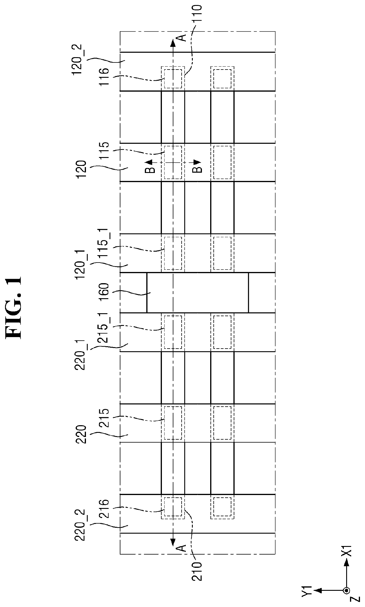
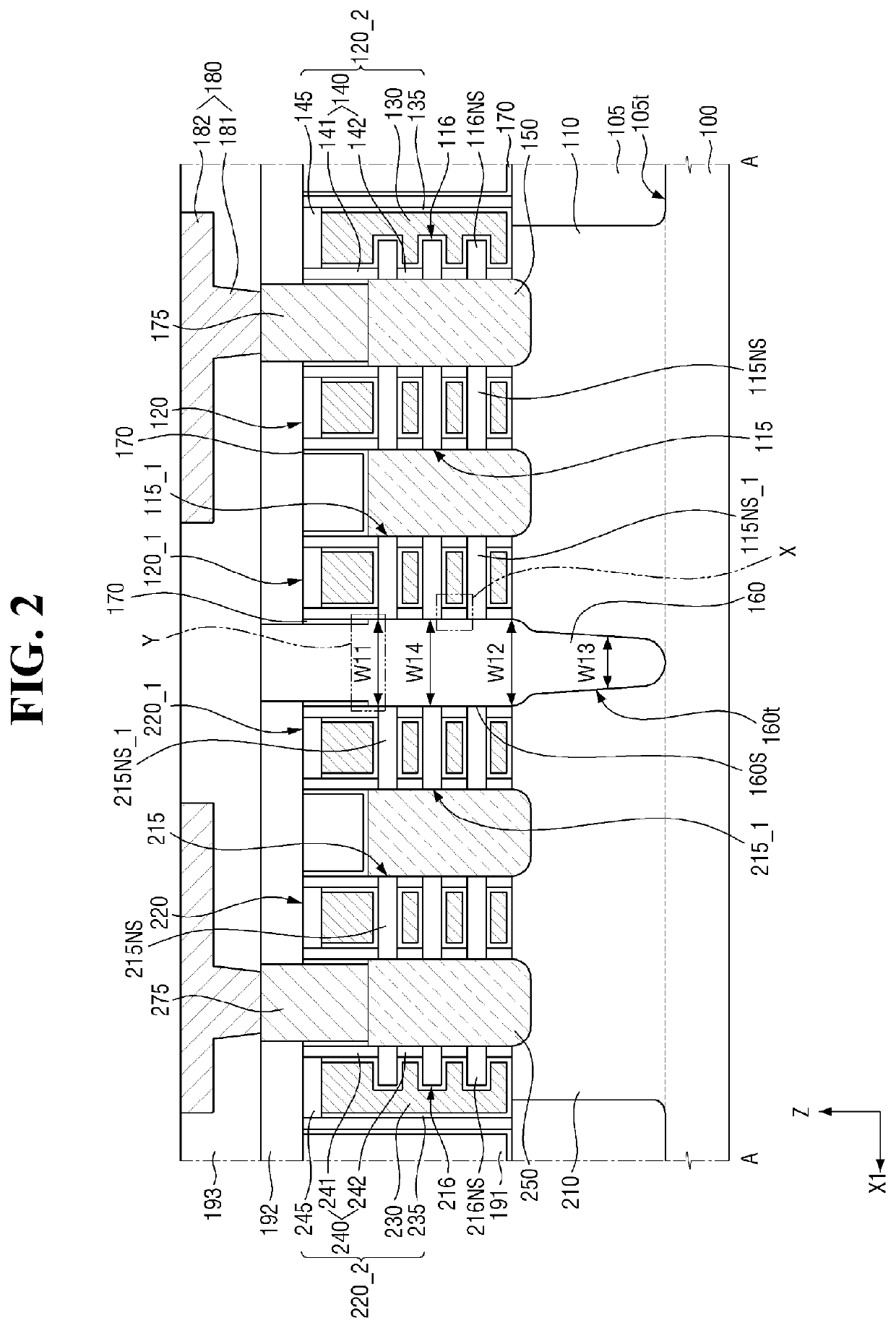
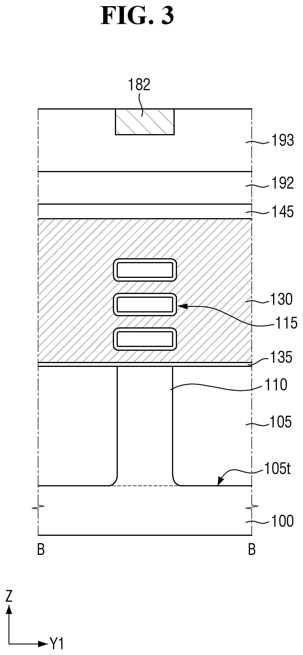
[0029]FIG. 1 is a plan view illustrating a semiconductor device according to an example embodiment. FIG. 2 is a cross-sectional view taken along line A-A of FIG. 1. FIG. 3 is a cross-sectional view taken along line B-B of FIG. 1. FIG. 4 is an enlarged view of portion X of FIG. 2. FIG. 5 is an enlarged view of portion Y of FIG. 2.

[0030]Referring to FIGS. 1 to 5, a semiconductor device according to an example embodiment may include a substrate 100, a first lower pattern 110, a second lower pattern 210, first active pattern stacks 115 and 115_1, a first fin-cut pattern stack 116, contacts 175 and 275, a wiring structure 180, interlayer insulation layers 191, 192, and 193, second active pattern stacks 215 and 215_1, a second fin-cut pattern stack 216, a second fin-cut pattern stack 216, first gate structures 120 and 120_1, second gate structures 220 and 220_1, a first fin-cut gate structure 120_2, a second fin-cut gate structure 220_2, and a first device isolation layer 160. (For conven...


PUM


Abstract

A semiconductor device includes a substrate, a first lower pattern and a second lower pattern on the substrate and arranged in a line in a first direction, a first active pattern stack disposed on and spaced apart from the first lower pattern, a second active pattern stack disposed on and spaced apart from the first lower pattern, a fin-cut gate structure disposed on the first lower pattern and overlapping a portion of the first lower pattern, a first gate structure surrounding the first active pattern stack and extending in a second direction crossing the first direction, a second gate structure surrounding the second active pattern stack and extending in the second direction, and a device isolation layer between the first gate structure and the second gate structure and separating the first lower pattern and the second lower pattern.

Description

CROSS-REFERENCE TO RELATED APPLICATION[0001]Korean Patent Application No. 10-2019-0091487, filed on Jul. 29, 2019, in the Korean Intellectual Property Office, and entitled: “Semiconductor Device,” is incorporated by reference herein in its entirety.BACKGROUND1. Field[0002]Embodiments relate to a semiconductor device.2. Description of the Related Art[0003]As a semiconductor device becomes more highly integrated, it becomes more difficult to implement a transistor performance required by a user. As such, various field effect transistors have been proposed. For example, a high dielectric layer-metal gate structure has been proposed instead of a general field effect transistor including a gate insulation layer and a gate electrode formed using silicon oxide and polysilicon, respectively.[0004]As a feature size of the field effect transistor is reduced, a length of a gate and a length of a channel thereunder become small. Thus, a manufacturing process and structure of an integrated circu...

Claims


Application Information

Patent Timeline
IPC IPC(8): H01L27/092H01L23/535H01L29/423
CPCH01L27/0924H01L29/42392H01L23/535H01L27/0886H01L29/785H01L29/7855H01L21/76232H01L29/78696H01L29/7831H01L29/7846H01L21/823828H01L21/823842H01L21/764
Inventor GWON, YEONG HANJEONG, SOO YEONBAE, GEUM JONGBAE, DONG IL
Owner SAMSUNG ELECTRONICS CO LTD
Why Eureka
Eureka Blog
Learn More