Method for manufacturing wiring board, and wiring board

Active Publication Date: 2021-03-18
TOYOTA JIDOSHA KK
View PDF0 Cites 2 Cited by
  • Summary
  • Abstract
  • Description
  • Claims
  • Application Information

AI Technical Summary

Benefits of technology

This patent describes a method for making a wiring board by placing ink containing metal nanoparticles on a surface and then sintering them to form a seed layer. This invention allows for the creation of a fine pattern of the seed layer, which is important for making the wiring board.

Problems solved by technology
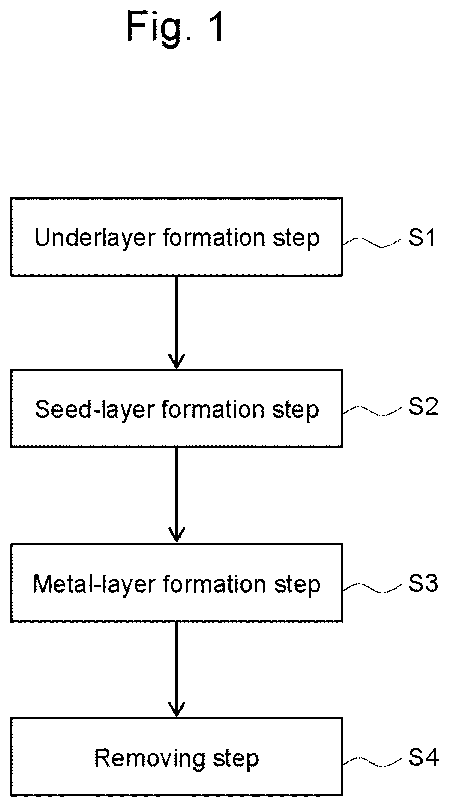
In this way this method has the problems that a lot of steps is required to form and remove the resist pattern and a lot of liquid waste is generated.
Such a fine seed layer means very small contact area between the metal layer and the seed layer if the metal layer is formed only on the surface of the seed layer, and this degrades the adhesion between the metal layer and the seed layer.

Method used


Image

  • Method for manufacturing wiring board, and wiring board
  • Method for manufacturing wiring board, and wiring board
  • Method for manufacturing wiring board, and wiring board

Examples


example 1

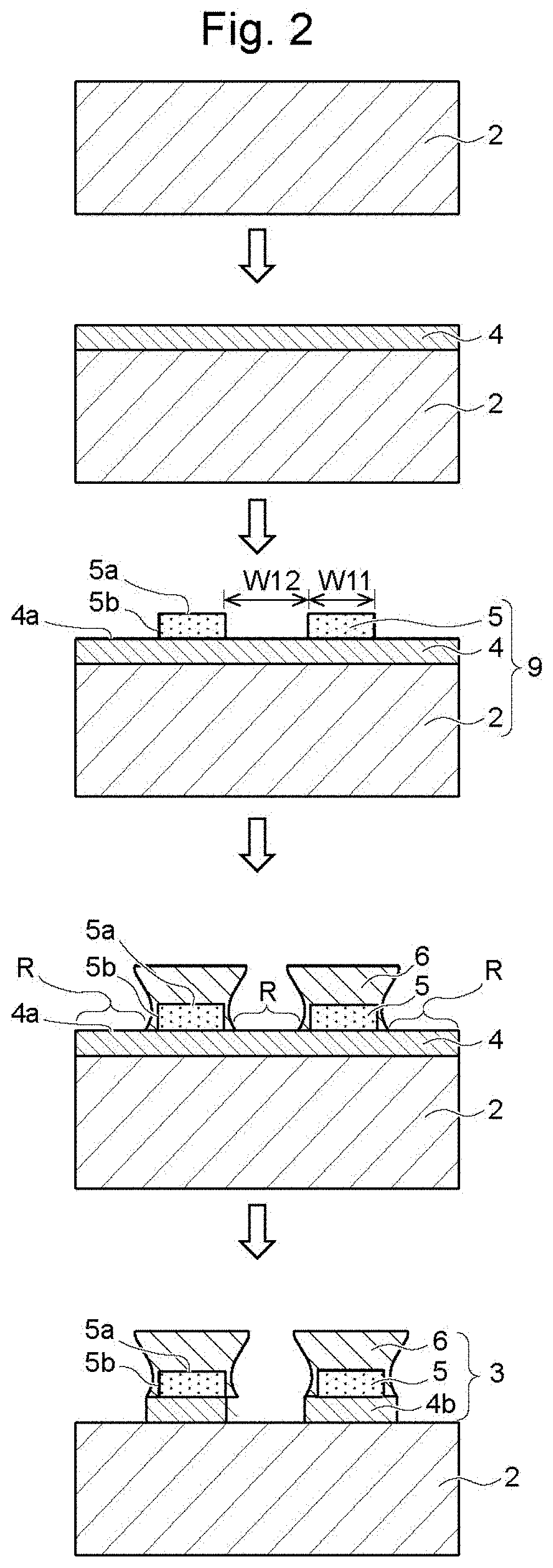
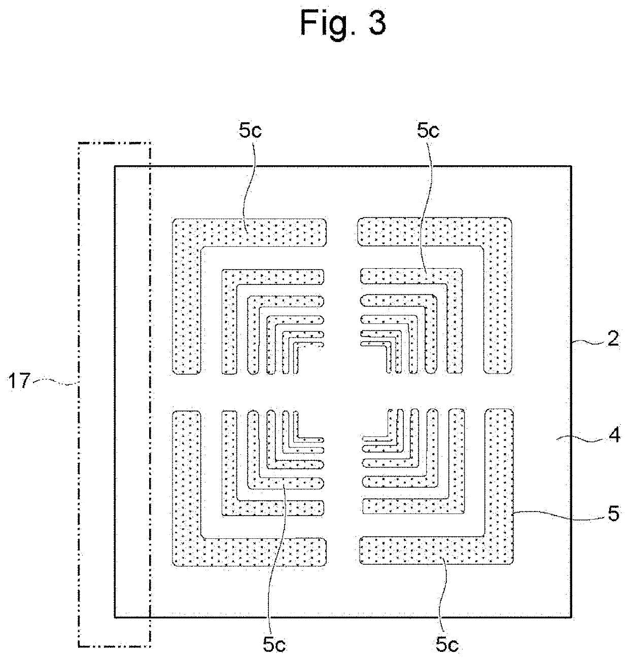
[0083]The wiring board 1 was manufactured by the above-described manufacturing method, using glass as the material of the substrate 2, WSi2 as the material of the underlayer 4, silver as the material of the seed layer 5, and copper as the material of the metal layer 6. Specifically, the underlayer 4 made of WSi2 was formed on the surface of a substrate 2 made of glass by sputtering using WSi2 as a target. At this time, the thickness of the underlayer 4 was 100 nm. Then, the seed layer 5 having the thickness of 100 nm was formed on the surface of the underlayer 4 using ink containing silver nanoparticles having the average particle diameter of 50 nm. At this time, the ink was disposed on the surface of the underlayer 4 by screen printing, and the silver nanoparticles were sintered at the temperature of 120° C. to form the seed layer 5. The seed layer 5 was formed to have a plurality of independent patterns 5c.

[0084]Next, the metal layer 6 was formed on the surface 5a of the seed lay...

example 2

[0086]The material of the underlayer 4 was ZrSi2. Otherwise, the manufacturing method was the same as in Example 1.

example 3

[0087]The material of the underlayer 4 was ITO. Otherwise, the manufacturing method was the same as in Example 1.


PUM

PropertyMeasurementUnit
Temperatureaaaaaaaaaa
Lengthaaaaaaaaaa
Lengthaaaaaaaaaa

Abstract

Provided is a method for manufacturing a wiring board that forms a wiring layer having favorable adhesion without a resin resist pattern. A method prepares a substrate with seed-layer including: a underlayer on the surface of an insulating substrate; and a seed layer on the surface of the underlayer, the seed layer having a predetermined pattern and containing metal; presses a solid electrolyte membrane against the seed layer and the underlayer, and applies voltage between an anode and the underlayer to reduce metal ions in the membrane and form a metal layer on the surface of the seed layer; and removes an exposed region without the seed layer and the metal layer of the underlayer to form a wiring layer including the underlayer, the seed layer and the metal layer on the surface of the substrate.

Description

CROSS REFERENCE TO RELATED APPLICATIONS[0001]The present application claims priority from Japanese patent application JP 2019-168980 filed on Sep. 18, 2019, the entire content of which is hereby incorporated by reference into this application.BACKGROUNDTechnical Field[0002]The present disclosure relates to methods for manufacturing a wiring board to form a wiring layer on the surface of a substrate, and wiring boards.Description of Related Art[0003]Conventionally known methods of manufacturing a wiring board includes a subtractive method, a semi-additive method, and a full-additive method. Among these manufacturing methods, a semi-additive method is mainly used for a high-density wiring board.[0004]JP 2016-225524 A, for example, discloses the method for manufacturing a wiring board by a semi-additive method. The method of JP 2016-225524 A stacks a dielectric layer, a seed layer, and a first plating layer in this order on the surface of a base layer (substrate), and forms a resist pa...

Claims


Application Information

Patent Timeline
IPC IPC(8): H05K3/38H05K3/24H05K3/20
CPCH05K3/388H05K3/205H05K3/241H05K3/182H05K3/383H05K2203/0502H05K3/243H05K3/108H05K3/242H05K3/246H05K2203/0713H05K2203/0716H05K2203/0723H05K2201/09827H05K2201/098H05K2201/09981H05K2201/0347H05K2201/0338H05K2201/0341H05K2201/0391C25D5/02C25D3/38C25D5/06C23C18/08H05K3/188H05K3/384H05K3/16C25D5/028H05K3/4007H05K3/423
Inventor OKAMOTO, KAZUAKIYANAGIMOTO, HIROSHIMORI, RENTARO
Owner TOYOTA JIDOSHA KK
Why Eureka
Try Eureka