
Plasma photonic crystals with integrated plasmonic arrays in a microtubular frame

a technology of plasmonic arrays and crystals, applied in the field of electromagnetic devices, can solve the problems of including the transmission and reflection spectra, and the inability to quickly change the electromagnetic properties of the crystal with time, so as to achieve the effect of increasing or suppressing crystal resonan

Active Publication Date: 2021-04-08
THE BOARD OF TRUSTEES OF THE UNIV OF ILLINOIS
View PDF20 Cites 0 Cited by
  • Summary
  • Abstract
  • Description
  • Claims
  • Application Information

AI Technical Summary

Benefits of technology

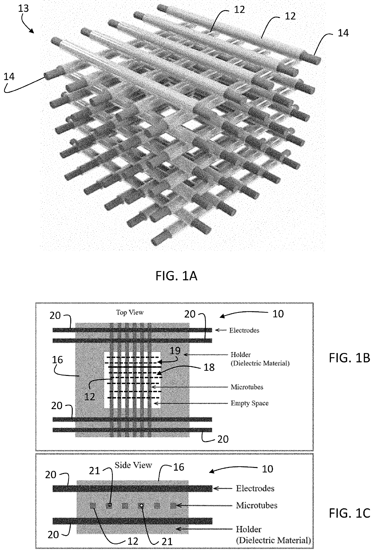
This patent is about a new way to reflect, transmit, and store incident electromagnetic energy. It involves creating a periodic array of microplasmas in small tubes, which are then confined within larger microtubes to form a photonic crystal. The spacing and electron density of the microtubes are designed to produce a unique response to the incident energy. The energy can be interacted with the microplasmas to produce resonance shifting or increased / suppressed crystal resonances. The crystal also includes electrodes to stimulate the microplasmas. The technical effect of this patent is an improved method for controlling the interaction of electromagnetic energy with a periodic array of microplasmas, allowing for better reflection and transmission of the energy.

Problems solved by technology

One drawback of conventional photonic crystals is that the properties of the crystal are fixed and not readily altered.
That is, the crystal is static and the electromagnetic properties of the crystal, including its transmission and reflection spectra, cannot be quickly varied with time.
Sakai et al. generated columnar plasmas ˜2 mm in diameter in a periodic, two-dimensional structure that had an overall area of 44 mm×44 mm, but converting this structure into three dimensions is problematic because of the electrode configuration and structure geometry.
The first of these concerns the non-uniform diameter of the columnar plasmas (nominally 2 mm in diameter), the overlap between (i.e., partial blending of) adjacent plasmas, and the limited precision in the positioning of the plasmas.
All of these factors limit the electromagnetic performance of the crystals and, specifically, the Q of the crystal resonances and their tunability.
The weak attenuation of incident electromagnetic energy, and the restriction of previous plasma photonic crystal designs to one or two dimensions suggest that the prior art does not offer structures capable of competing with photonic crystals fabricated from solids, or for capturing the inherent advantages that plasma-based photonic crystals have with respect to tunability and reconfigurability.
The devices of the '210 Patent do, however, exhibit significant insertion loss which is introduced by the polymer enclosure for the photonic crystal.
This insertion loss can be an impediment to the application of these devices in 5G communications systems, for example.
Another limitation is that the volume between microplasmas is occupied by polymer (or other material from which the array enclosure is fabricated), thus precluding the insertion of electromagnetically-active materials or structures (other than the plasma crystal itself) between the microchannels fabricated in the polymer block (enclosure).
In addition, the inability to surround each microplasma, or groups of microplasmas, with other electromagnetically-active media or structures limits the utility of the '210 Patent for communications and sensor applications.

Method used


Image

  • Plasma photonic crystals with integrated plasmonic arrays in a microtubular frame
  • Plasma photonic crystals with integrated plasmonic arrays in a microtubular frame
  • Plasma photonic crystals with integrated plasmonic arrays in a microtubular frame

Examples


Embodiment Construction

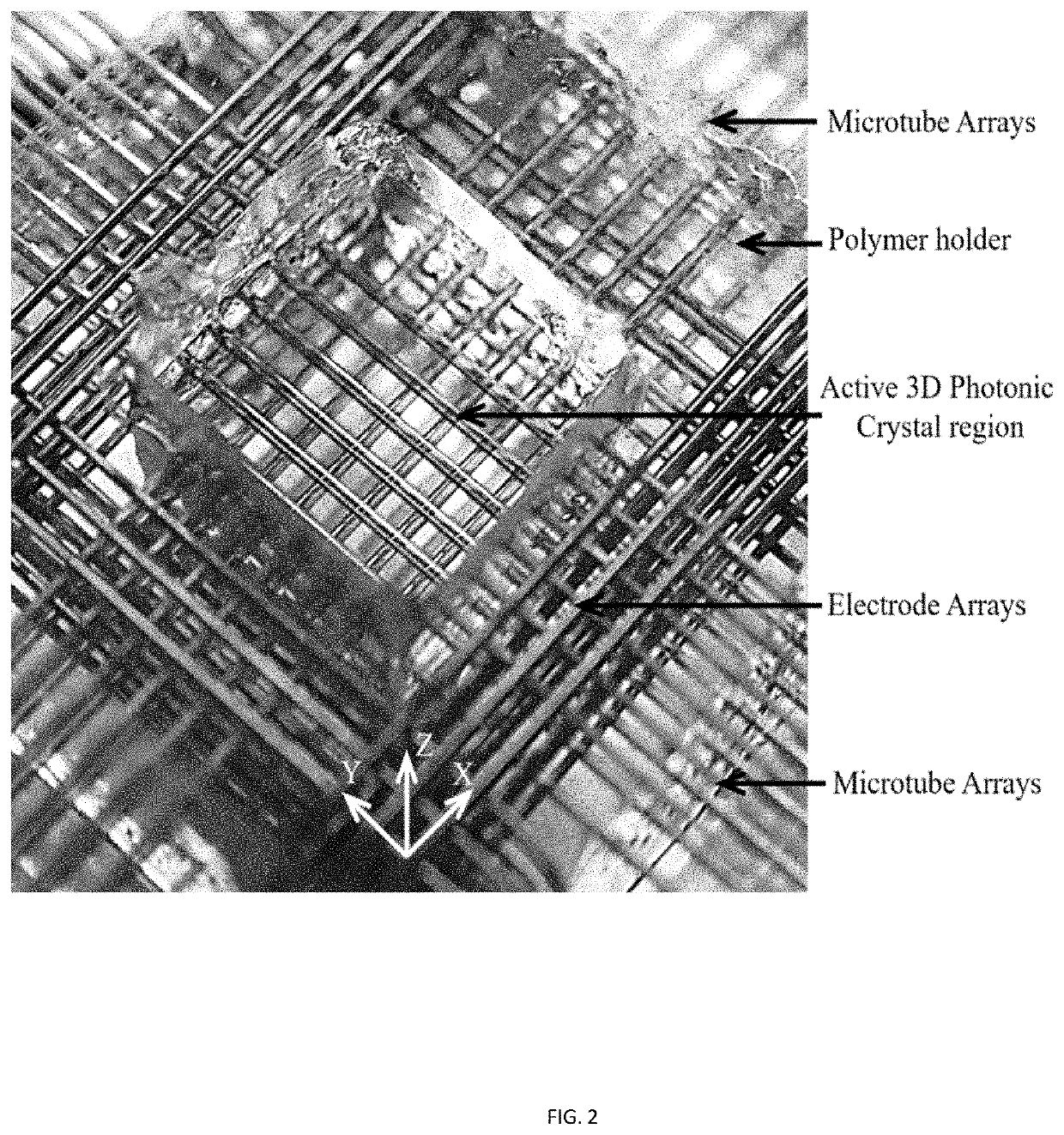
[0024]Preferred embodiments provide a microplasma photonic crystal device that is capable of limiting insertion losses and incorporating electromagnetically-active materials or structures among the microplasmas in the periodic crystal structure of the device. Prototypes have been constructed that include complex, three-dimensional (3D) structures of free-standing arrays of polyimide microtubes. The microtubes are assembled into a 3D-printed polymer scaffold supported by a holder / mold situated around the perimeter of the scaffold, which results in structures that are dimensionally precise without distorting the diameter, or altering the position, of the individual microtubes. The elimination of the bulk polymer enclosure of U.S. Pat. No. 10,548,210 reduces the insertion loss of the crystal by tens of dB.

[0025]In a preferred embodiment, portions of the outer wall of the microtubes are partially coated, for example with a metal. The coating of the microtubes with specific metals such a...


PUM

PropertyMeasurementUnit
interior volumeaaaaaaaaaa
inner diameteraaaaaaaaaa

Abstract

The invention provides a microplasma photonic crystal for reflecting, transmitting and / or storing incident electromagnetic energy includes a periodic array of elongate microtubes confining microplasma therein and having a column-to-column spacing, average electron density and plasma column diameter selected to produce a photonic response to the incident electromagnetic energy entailing the increase or suppression of crystal resonances and / or shifting the frequency of the resonances. The crystal also includes electrodes for stimulating microplasma the elongated microtubes Electromagnetic energy can be interacted with the periodic array of microplasma to reflect, transmit and / or trap the incident electromagnetic energy.

Description

PRIORITY CLAIM AND REFERENCE TO RELATED APPLICATION[0001]The application claims priority under 35 U.S.C. § 119 and all applicable statutes from prior U.S. provisional application Ser. No. 62 / 898,112, which was filed Sep. 10, 2019.STATEMENT OF GOVERNMENT INTEREST[0002]This invention was made with government support under grant no. FA9550-14-1-0002 awarded by the U.S. Air Force Office of Scientific Research. The government has certain rights in the invention.FIELD[0003]Fields of the invention include electromagnetic devices, including resonators, filters, phase shifters, beamsplitters, routers, two- and three-dimensional photonic crystals, and microplasma devices. Example applications include the re-directing (reflecting) or storing and release of electromagnetic energy, including electromagnetic energy in the microwave, mm-wave, or THz spectral regions (˜1 GHz-10 THz). Specific examples of devices enabled by the invention include bandpass filters, beamsplitters or routers, attenuator...

Claims


Application Information

Patent Timeline
Patent Type & Authority Applications(United States)
IPC IPC(8): H05H1/24
CPCH05H1/2406H05H2001/2437H05H2001/2431H05H2001/2412H05H1/2431H05H1/2437H05H1/2418
Inventor EDEN, J. GARYSUN, PETER P.CHEN, WENYUANHUANG, YIN
Owner THE BOARD OF TRUSTEES OF THE UNIV OF ILLINOIS
Learn More