
Methods for selective deposition of doped semiconductor material

a semiconductor material and selective deposition technology, applied in the direction of polycrystalline material growth, crystal growth process, chemically reactive gas, etc., can solve the problems of high boron concentration, low contact resistance of conventional device scaling techniques, and significant challenges for future technology nodes

Active Publication Date: 2021-04-22
ASM IP HLDG BV
View PDF0 Cites 146 Cited by
  • Summary
  • Abstract
  • Description
  • Claims
  • Application Information

AI Technical Summary

Benefits of technology

The present patent relates to a method and apparatus for selectively depositing doped semiconductor layers with low contact resistance. The method can involve selectively depositing a first doped semiconductor layer over a first material, selectively depositing a second doped semiconductor layer over the first doped semiconductor layer, without the need for annealing to improve contact resistance. The doped semiconductor layers can be formed at relatively low temperatures, such as 350°C to 600°C. The method can be performed in the same reaction chamber or different reaction chambers. The structures formed using the method can include a substrate with a surface including different materials, and the doped semiconductor layers can be used to form a source or drain region of a device, such as a field effect transistor. The method and apparatus can provide improved selectivity and efficiency in depositing doped semiconductor layers.

Problems solved by technology

However, conventional device scaling techniques face significant challenges for future technology nodes.
In some cases, boron may have relatively low solubility in the semiconductor material, and thus high concentrations of the p-type dopant and thus low contact resistance to the semiconductor material can be difficult to obtain.
However, high boron concentrations are difficult to achieve with higher Ge:Si ratios due to the low boron solubility in germanium, and therefore, attempts to simply increase the boron concentration in the silicon germanium film have generally not been sufficient to decrease the contact resistivity of the silicon germanium layers to desired values.
Such techniques may be problematic because the use of the relatively high temperatures during the anneal process can lead to clustering of one or more of the dopants of the doped semiconductor films.
However, such techniques may not be well developed.

Method used


Image

  • Methods for selective deposition of doped semiconductor material
  • Methods for selective deposition of doped semiconductor material
  • Methods for selective deposition of doped semiconductor material

Examples


Embodiment Construction

[0044]The description of exemplary embodiments of methods, structures, devices and systems provided below is merely exemplary and is intended for purposes of illustration only; the following description is not intended to limit the scope of the disclosure or the claims. Moreover, recitation of multiple embodiments having stated features is not intended to exclude other embodiments having additional features or other embodiments incorporating different combinations of the stated features. For example, various embodiments are set forth as exemplary embodiments and may be recited in the dependent claims. Unless otherwise noted, the exemplary embodiments or components thereof may be combined or may be applied separate from each other.

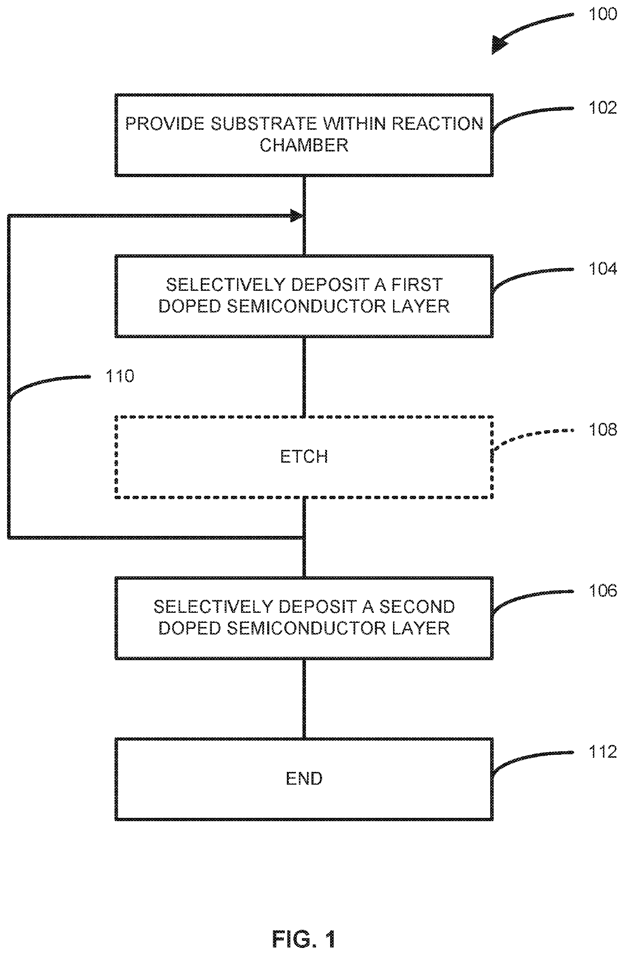
[0045]As set forth in more detail below, various embodiments of the disclosure provide methods for selectively depositing doped semiconductor material on a surface of a substrate. Exemplary methods can be used to, for example, form source and / or drain regio...


PUM

PropertyMeasurementUnit
thicknessaaaaaaaaaa
thicknessaaaaaaaaaa
carrier densityaaaaaaaaaa

Abstract

Methods and systems for selectively depositing material, such as doped semiconductor material, are disclosed. An exemplary method includes providing a substrate, comprising a first area comprising a first material and a second area comprising a second material, selectively depositing a first doped semiconductor layer overlying the first material relative to the second material and selectively depositing a second doped semiconductor layer overlying the first doped semiconductor layer relative to the second material.

Description

CROSS-REFERENCE TO RELATED APPLICATIONS[0001]This application claims priority to U.S. Provisional Patent Application Ser. No. 62 / 916,662 filed Oct. 17, 2019 titled METHODS FOR SELECTIVE DEPOSITION OF DOPED SEMICONDUCTOR MATERIAL, the disclosure of which is hereby incorporated by reference in its entirety.FIELD OF INVENTION[0002]The present disclosure generally relates to methods and systems suitable for forming electronic devices. More particularly, the disclosure relates to methods and systems that can be used for selectively depositing material, such as doped semiconductor material, on a surface of a substrate.BACKGROUND OF THE DISCLOSURE[0003]The scaling of semiconductor devices, such as, for example, complementary metal-oxide-semiconductor (CMOS) devices, has led to significant improvements in speed and density of integrated circuits. However, conventional device scaling techniques face significant challenges for future technology nodes.[0004]One approach to improve semiconducto...

Claims


Application Information

Patent Timeline
Patent Type & Authority Applications(United States)
IPC IPC(8): H01L21/02H01L29/08C23C16/455
CPCH01L21/02579H01L21/02488H01L21/02381C23C16/455H01L21/02532H01L29/0843H01L21/02384H01L21/0262H01L21/0245H01L21/02452H01L21/02535H01L21/02639C23C16/04C23C16/24C23C16/30C23C16/45523C23C16/56H01L21/02636H01L21/0251H01L21/823418C30B25/165C30B29/06
Inventor BARBOSA LIMA, LUCAS PETERSENKHAZAKA, RAMIXIE, QI
Owner ASM IP HLDG BV
Features
  • Generate Ideas
  • Intellectual Property
  • Life Sciences
  • Materials
  • Tech Scout
  • Unparalleled Data Quality
  • Higher Quality Content
  • 60% Fewer Hallucinations
Learn More