Organic el device as well as display apparatus, image pickup apparatus, communication apparatus, lighting apparatus, luminaire, and moving body each including the same

a technology of organic el and display apparatus, which is applied in the direction of semiconductor devices for light sources, lighting and heating devices, television systems, etc., can solve the problems of material degradation, exciton quenching, and insufficient durability of organic el devices disclosed in patent literature 1 to achieve good emission balance and improve durability

Pending Publication Date: 2021-04-29
CANON KK
View PDF0 Cites 0 Cited by
  • Summary
  • Abstract
  • Description
  • Claims
  • Application Information

AI Technical Summary

Benefits of technology

[0011]The present invention has been made to solve such problems and provides an organic EL device with improved durability and good emission balance and various apparatuses including the organic EL device.

Problems solved by technology

However, the organic EL device disclosed in Patent Literature 1 had insufficient durability.
Thus, positive holes are accumulated in the intermediate layer between two light-emitting layers, possibly causing exciton quenching due to the accumulated charge and material degradation due to charge accumulation.
Thus, energy transfer from a green- or blue-light-emitting layer on the opposite side of the first intermediate layer from the red-light-emitting layer is likely to occur to the red-light-emitting layer via the first intermediate layer, and energy transfer can be accompanied with a change in emission balance and a decrease in luminous efficiency.
Depending on the material structure, the intermediate layers may cause a decrease in device efficiency or may cause device degradation.

Method used


Image

  • Organic el device as well as display apparatus, image pickup apparatus, communication apparatus, lighting apparatus, luminaire, and moving body each including the same
  • Organic el device as well as display apparatus, image pickup apparatus, communication apparatus, lighting apparatus, luminaire, and moving body each including the same
  • Organic el device as well as display apparatus, image pickup apparatus, communication apparatus, lighting apparatus, luminaire, and moving body each including the same

Examples


exemplary embodiment 1

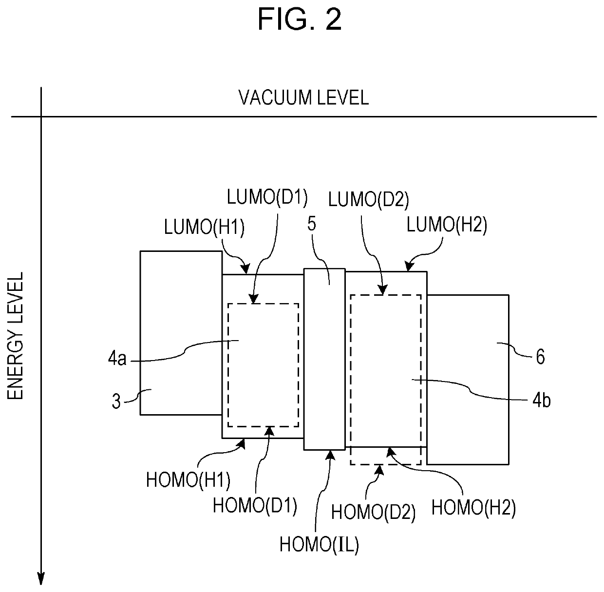
[0187]The HOMO and LUMO levels of hosts, dopants, and intermediate layer materials were measured by the following method. Table 1 shows the results.

A) Measurement of HOMO Level

[0188]Thin films 30 nm in thickness were formed from various materials on an aluminum substrate. HOMO levels in the thin films were measured with AC-3 (manufactured by Riken Keiki Co., Ltd.). Tables 1 and 2 show the results.

B) Measurement of LUMO Level

[0189]Thin films 30 nm in thickness were formed from various materials on a quartz substrate. The optical band gap (absorption edge) of a material to be measured in the thin films was determined with a spectrophotometer (“V-560” manufactured by JASCO Corporation). The sum of the optical band gap and the HOMO level was defined as the LUMO level.

Tables 1 and 2 show the results.

[0190]Tables 1 and 2 also show values calculated by a molecular orbital calculation method. A comparison with actual values shows that the HOMO level correlates with the LUMO level. In the pr...

exemplary embodiment 2

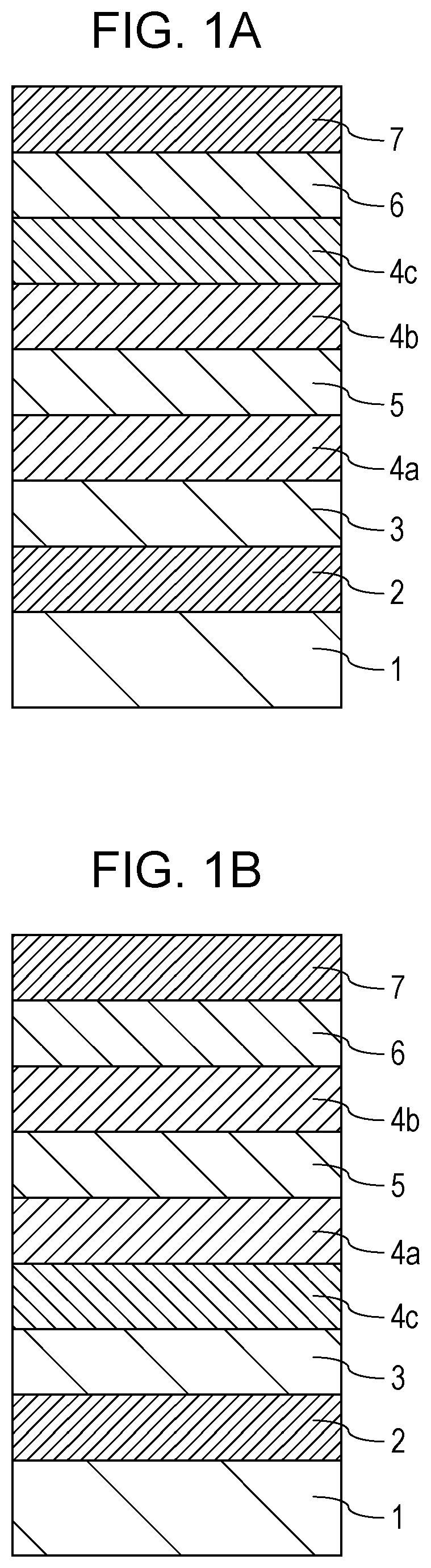
[0191]An organic EL device of the top emission type produced in the present exemplary embodiment included an anode, a hole-injection layer, a hole-transport layer, an electron-blocking layer, a first light-emitting layer, an intermediate layer, a second light-emitting layer, a hole-blocking layer, an electron-transport layer, an electron-injection layer, and a cathode on a substrate. More specifically, first, a 40-nm Ti film was formed on a glass substrate by sputtering and was patterned by photolithography to form an anode. The facing areas of the anode and the cathode were set to 3 mm2. Subsequently, the substrate on which up to a cleaned electrode was formed and a material were mounted in a vacuum evaporator (manufactured by ULVAC, Inc.), which was then evacuated to 1.33×10⁻⁴ Pa (1×10⁻⁶ Torr). UV / ozone cleaning was then performed. Subsequently, each layer of a layer structure shown in the following table 3 was formed.

TABLE 3ThicknessMaterial[nm]Electron-ET2:Cs (Mass ratio ET2:Cs ...

exemplary embodiments 12 to 14

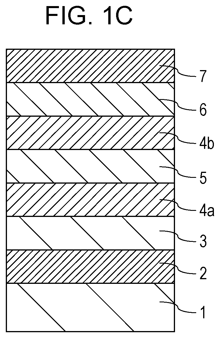
[0199]An organic EL device was produced in the same manner as in Exemplary Embodiment 2 except that the first light-emitting layer / intermediate layer / second light-emitting layer in Exemplary Embodiment 2 was changed to a layered structure of the first light-emitting layer / intermediate layer / second light-emitting layer / third light-emitting layer shown in Table 6 and that the compounds and concentrations were changed as shown in Table 6. The thicknesses of the first light-emitting layer / intermediate layer / second light-emitting layer / third light-emitting layer were 10 nm / 5 nm / 10 nm / 5 nm. The characteristics of the organic EL device were measured and evaluated in the same manner as in Exemplary Embodiment 2. Table 7 shows the results.

TABLE 6IntermediateFirst light-emitting layerlayerSecond light-emitting layerFirstFirstIntermediateSecondhostdopantlayer materialhostHOMOLUMOHOMOLUMOHOMOLUMOHOMOLUMO(H1)(H1)(D1)(D1)Mass(IL)(IL)(H2)(H2)[eV][eV][eV][eV]ratio[eV][eV][eV][eV]Example 12EM1RD5EM1...


PUM

PropertyMeasurementUnit
excited singlet energy levelaaaaaaaaaa
energyaaaaaaaaaa
energyaaaaaaaaaa

Abstract

An organic EL device includes at least an anode, a first light-emitting layer, an intermediate layer, a second light-emitting layer, and a cathode in this order. The intermediate layer is adjacent to the first light-emitting layer and the second light-emitting layer. The first light-emitting layer and the second light-emitting layer can trap electrons. A material constituting the intermediate layer is a hydrocarbon that has a HOMO level equal to or lower than the HOMO level of a host of the first light-emitting layer and that has a high S1 level.

Description

CROSS-REFERENCE TO RELATED APPLICATIONS[0001]This application is a Continuation of International Patent Application No. PCT / JP2019 / 025944, filed Jun. 28, 2019, which claims the benefit of Japanese Patent Application No. 2018-128017, filed Jul. 5, 2018, and Japanese Patent Application No. 2019-117143, filed Jun. 25, 2019, all of which are hereby incorporated by reference herein in their entirety.TECHNICAL FIELD[0002]The present invention relates to an organic EL device that emits light upon energization of an organic electroluminescence (EL) layer including a light-emitting layer between a pair of electrodes and various apparatuses including the organic EL device.BACKGROUND ART[0003]In recent years, research and development of full-color light-emitting arrays including an organic EL device has been energetically promoted. Full-color light-emitting arrays are produced by differently coloring a light-emitting layer for each pixel (device) or by using an organic EL device whose light-em...

Claims


Application Information

Patent Timeline
Patent Type & Authority Applications(United States)
IPC IPC(8): H01L51/50H04N5/225H01L51/52F21V3/00F21S43/145
CPCH01L51/5004H04N5/22525H01L51/5044H01L51/0097F21V3/00F21S43/145H01L2251/552H01L51/5278F21Y2115/15H04N23/53H10K85/622H10K85/624H10K85/626H10K50/11H10K2101/40H10K50/131H10K50/13H10K2101/30H10K50/19H10K59/12H10K77/111H10K85/623H10K85/633H10K85/6574H10K85/6576H10K2102/311
Inventor MIYASHITA, HIROKAZUTAKAYA, ITARUITO, TAKAYUKITAKAHIRA, MOEYAMAGUCHI, TOMONASHIOBARA, SATORUKOTAKE, TOMOKAZUIIDA, HARUNAYAMADA, NAOKIKAMATANI, JUN
Owner CANON KK
Why Eureka
Try Eureka