Organic electroluminescent element
a technology of electroluminescent elements and organic materials, applied in the field of organic electroluminescent elements, can solve problems such as the technical problem of prolonging the lifespan, and achieve the effects of reducing the leakage of excitons and charges, improving the characteristics of elements, and increasing the durability of materials used
- Summary
- Abstract
- Description
- Claims
- Application Information
AI Technical Summary
Benefits of technology
Problems solved by technology
Method used
Image
Examples
example 1
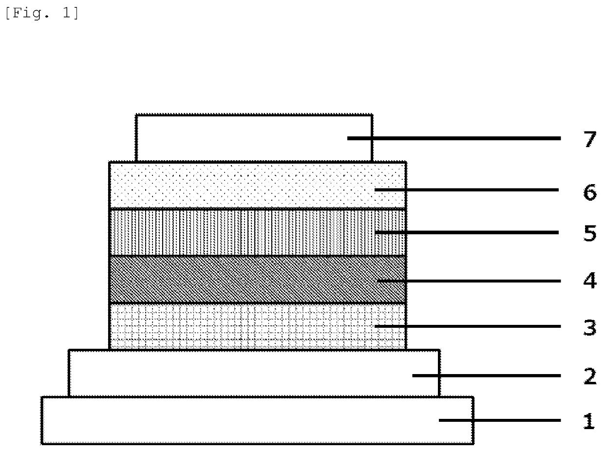
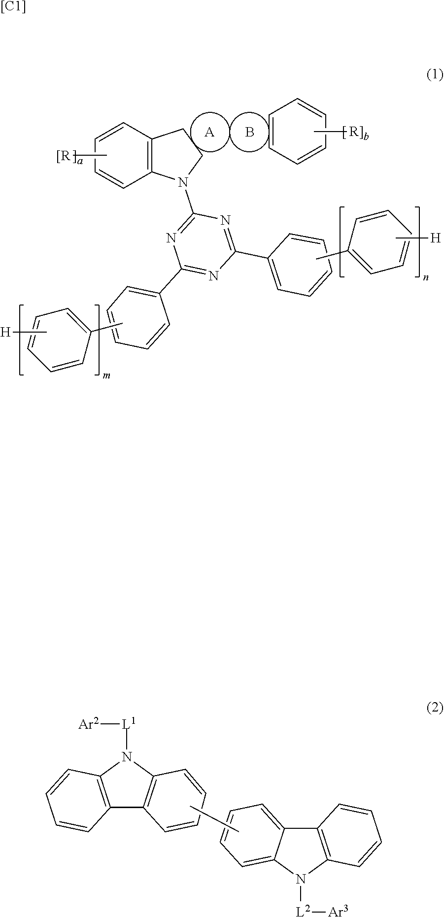
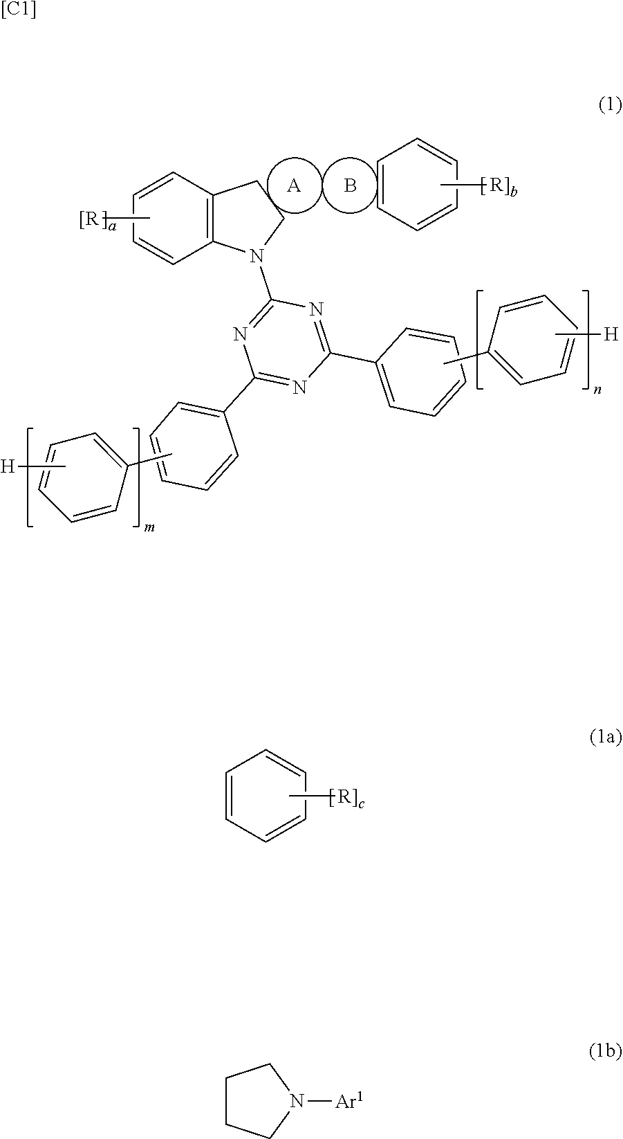
[0099]On a glass substrate on which an anode made of ITO with a film thickness of 110 nm was formed, respective thin films were laminated using a vacuum evaporation method at a degree of vacuum of 4.0×10⁻⁵ Pa. First, HAT-CN was formed with a thickness of 25 nm as a hole injection layer on ITO, and next NPD was formed with a thickness of 30 nm as a hole transport layer. Next, HT-1 was formed with a thickness of 10 nm as an electron blocking layer. Then, Pre-mixture H1 as a host and Ir(ppy)3 as a light-emitting dopant were co-vapor-deposited from different vapor deposition sources to form a light-emitting layer with a thickness of 40 nm. In this case, co-vapor-deposition was performed under vapor deposition conditions such that the concentration of Ir(ppy)3 was 10 wt %. Next, ET-1 was formed with a thickness of 20 nm as an electron transport layer. In addition, lithium fluoride (LiF) was formed with a thickness of 1 nm as an electron injection layer on the electron transport layer. Fi...
examples 2 to 15
[0100]Organic EL elements were produced in the same manner as in Example 1 except that any of Pre-mixtures H2 to H15 was used as the host in Example 1.
example 16
[0101]An organic EL element was produced in the same manner as in Example 1 except that, in Example 1, a light-emitting layer was formed using Pre-mixture H1 as a host and Ir(ppy)3 as a light-emitting dopant, and Compound C was then formed with a thickness of 10 nm as a hole blocking layer on the light-emitting layer, and next ET-1 was formed with a thickness of 10 nm as the electron transport layer.
PUM
| Property | Measurement | Unit |
|---|---|---|
| weight reduction temperatures | aaaaa | aaaaa |
| internal quantum efficiency | aaaaa | aaaaa |
| internal quantum efficiency | aaaaa | aaaaa |
Abstract
Description
Claims
Application Information


