

Circuit design assistance system and computer readable medium
a technology of circuit design applied in the field of circuit design assistance system and computer readable medium, can solve the problem that the power consumption associated with the occurrence of glitches cannot be ignored
- Summary
- Abstract
- Description
- Claims
- Application Information
AI Technical Summary
Benefits of technology
Problems solved by technology
Method used
Image

Examples
first embodiment
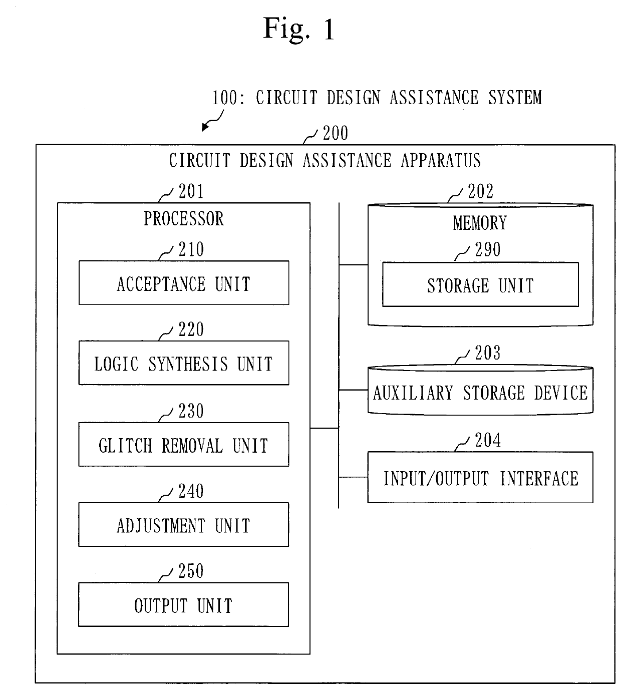
[0039]A circuit design assistance system 100 will be described based on FIGS. 1 to 8.
Description of Configuration
[0040]Based on FIG. 1, a configuration of the circuit design assistance system 100 and a configuration of a circuit design assistance apparatus 200 will be described.
[0041]The circuit design assistance system 100 includes the circuit design assistance apparatus 200.
[0042]The circuit design assistance apparatus 200 may be realized by two or more apparatuses.
[0043]The circuit design assistance apparatus 200 is a computer that includes hardware, such as a processor 201, a memory 202, an auxiliary storage device 203, and an input / output interface 204. These hardware components are connected with one another via signal lines.
[0044]The processor 201 is an integrated circuit (IC) that performs operational processing, and controls other hardware components. For example, the processor 201 is a central processing unit (CPU), a digital signal processor (DSP), or a graphics processin...
second embodiment
[0148]With regard to an embodiment in which the accuracy of detecting a glitch occurrence place is enhanced, differences from the first embodiment will be mainly described based on FIG. 9
Description of Configuration
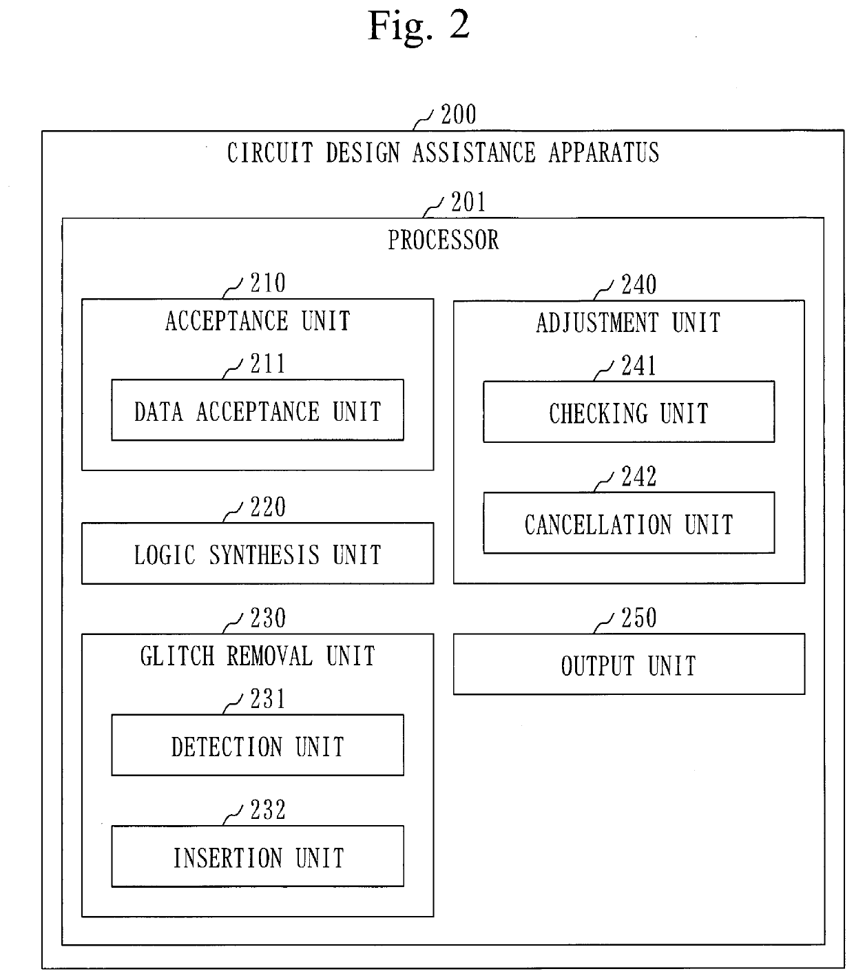
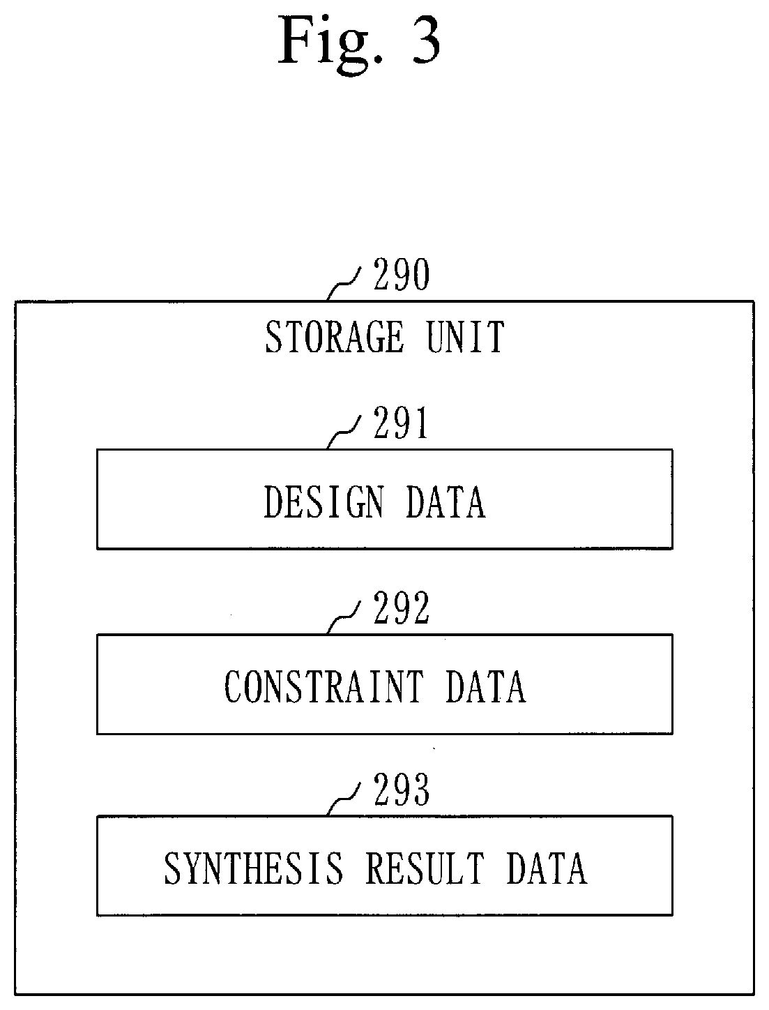
[0149]The configuration of the circuit design assistance system 100 is the same as the configuration in the first embodiment (see FIGS. 1 to 3).
Description of Operation
[0150]The overall flow of the circuit design assistance method is the same as the flow in the first embodiment (see FIG. 4).
[0151]However, a detection process (S130) is different from the process in the first embodiment.
[0152]In step S130, the detection unit 231 detects one or more predicted places in the target circuit, based on the synthesis result data 293.
[0153]A predicted place is a place where a glitch is predicted to occur.
[0154]Specifically, the detection unit 231 counts the number of applicable paths for each combinational circuit as the number of input signals of each combinational circuit.
[0155]A...
third embodiment
[0165]With regard to an embodiment in which places where glitch removal circuits are inserted are optimized, differences from the first and second embodiments will be mainly described based on FIG. 10.
Description of Configuration
[0166]The configuration of the circuit design assistance system 100 is the same as the configuration in the first embodiment (see FIGS. 1 to 3).
Description of Operation
[0167]The overall flow of the circuit design assistance method is the same as the flow in the first embodiment (see FIG. 4).
[0168]However, the detection process (S130) is different from the process in the first embodiment.
[0169]In step S130, the detection unit 231 detects one or more predicted places in the target circuit, based on the synthesis result data 293.
[0170]A predicted place is a place where a glitch is predicted to occur.
[0171]Specifically, the detection unit 231 counts applicable paths for each combinational circuit as the number of input signals of each combinational circuit, as d...
PUM
 Abstract
Description
Claims
Application Information