
Terminal protection circuit of semiconductor chip

Active Publication Date: 2021-07-22
FUJI ELECTRIC CO LTD
View PDF0 Cites 0 Cited by
  • Summary
  • Abstract
  • Description
  • Claims
  • Application Information

AI Technical Summary

Benefits of technology

This patent describes a circuit that helps protect the terminals of a semiconductor chip. It includes a ground terminal, a chip-peripheral ground line that connects to the ground terminal, and an overcurrent sensing circuit. The overcurrent sensing circuit includes a comparator, a threshold voltage generator, and a potential shift element. The potential shift element adjusts the threshold voltage based on the potential at a certain point on the chip-peripheral ground line. The technical effect of this patent is to provide a more precise and effective way to protect the terminals of a semiconductor chip from overcurrent events.

Problems solved by technology

As a result, the capacitor Cfo connected to the CFO terminal starts being charged, which results in an increase in the voltage V_CFO of the CFO terminal.
However, according to the technique disclosed in Japanese Laid-open Patent Publication No. 2013-062721, thresholds of a comparator used to detect overcurrent are changed according to the magnitudes of an average load current, an alternating current change of the load current, and a power source voltage, and thus there remains the problem of not being able to cause the thresholds to respond in the event of instantaneous disturbances such as noise.

Method used


Image

  • Terminal protection circuit of semiconductor chip
  • Terminal protection circuit of semiconductor chip
  • Terminal protection circuit of semiconductor chip

Examples


Embodiment Construction

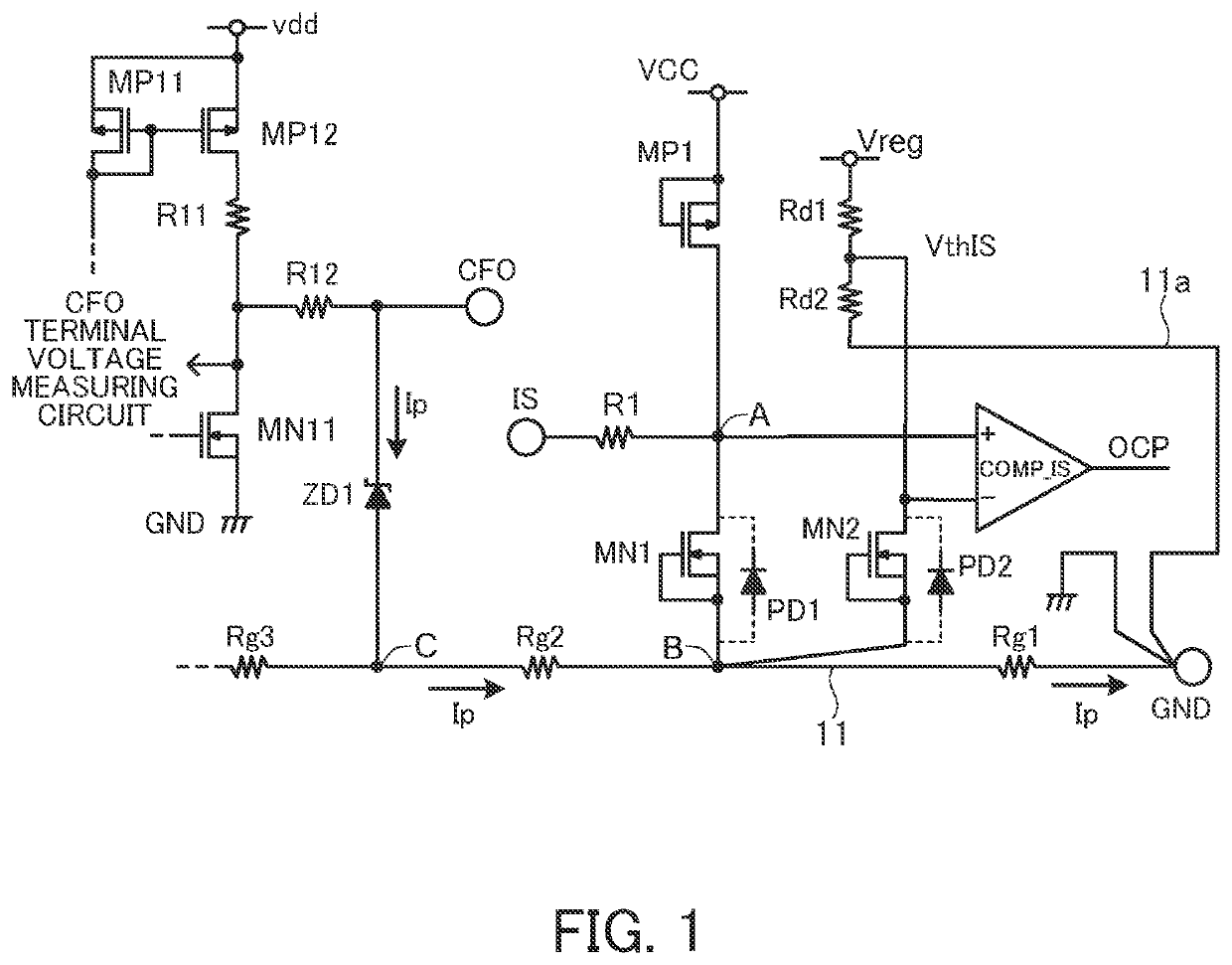
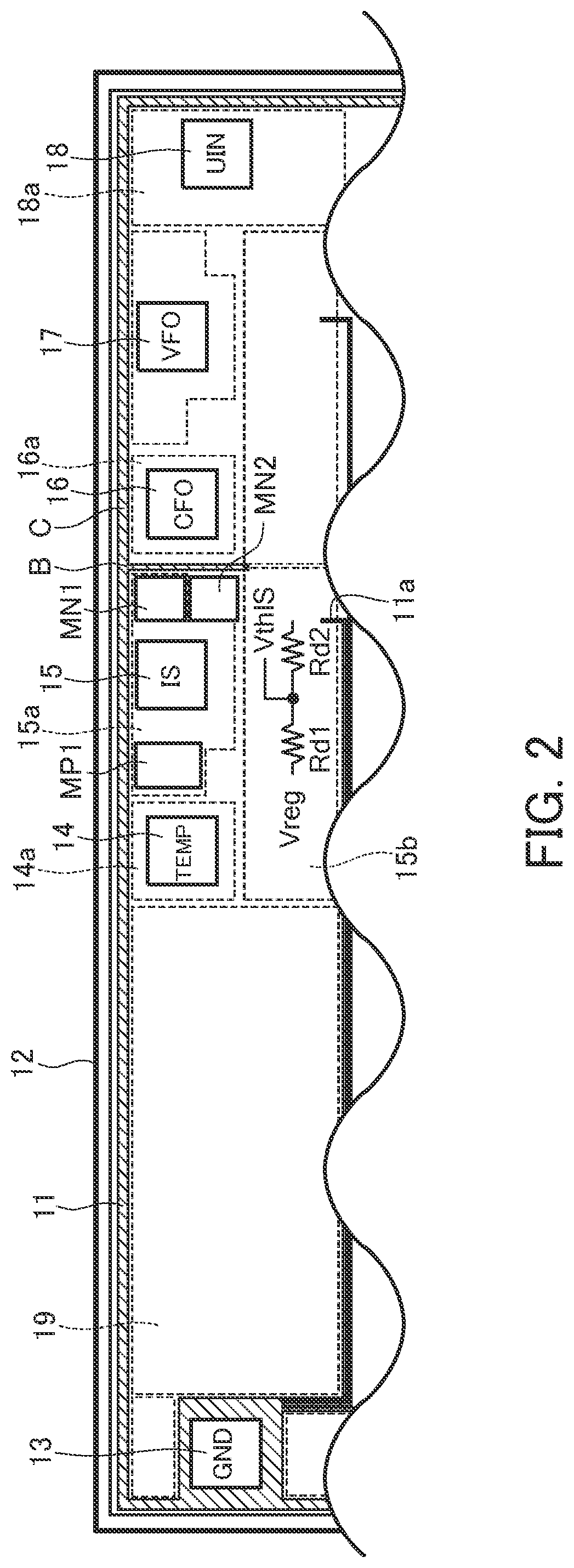
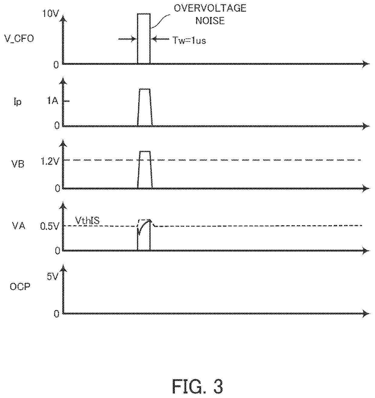
[0044]An embodiment being applied to a low-voltage side control circuit having an overcurrent sensing circuit located away from a pad of a GND terminal along a chip-peripheral ground line will be described below in detail with reference to the accompanying drawings. Note that, in the following description, the low-voltage side control circuit and an IPM including the low-voltage side control circuit are explained with reference to FIG. 4, and like reference numerals are given to like components illustrated in FIGS. 5 and 6 used to explain the conventional technique above.

[0045]FIG. 1 illustrates exemplary circuit geometry with terminal protection circuits of a low-voltage side control circuit according to an embodiment. FIG. 2 illustrates an exemplary arrangement on a semiconductor chip of the low-voltage side control circuit. FIG. 3 illustrates operation waveforms of the terminal protection circuits in response to application of an overvoltage. Note that FIG. 3 depicts, from the to...


PUM


Abstract

A terminal protection circuit of a semiconductor chip, including a first pad serving as a ground terminal of the semiconductor chip, a ground line extending along an outer periphery of the semiconductor chip and being connected to the first pad, and an overcurrent sensing circuit. The overcurrent sensing circuit has a second pad, a threshold voltage generating circuit, a comparator having inverting and non-inverting input terminals respectively connected to the threshold voltage generating circuit and the second pad, the comparator comparing a current detection signal and a threshold voltage received respectively at the non-inverting and inverting input terminals, a first input protection element connected between the second pad and a first position on the chip-peripheral ground line, and a potential shift element connected between the inverting input terminal of the comparator and the first position, for shifting the threshold voltage thereat according to a potential at the first position.

Description

CROSS-REFERENCE TO RELATED APPLICATION[0001]This application is based upon and claims the benefit of priority of the prior Japanese Patent Application No. 2020-005547, filed on Jan. 17, 2020, the entire contents of which are incorporated herein by reference.BACKGROUND OF THE INVENTION1. Field of the Invention[0002]The embodiment discussed herein relates to a terminal protection circuit of a semiconductor chip.2. Background of the Related Art[0003]Three-phase motors used in, for example, compressors of air conditioners are driven and controlled by motor drive devices. Such a motor drive device is a single package incorporating together power switches for controlling power to the three-phase motor, drive circuits for driving on and off the power switches, and various protection circuits.[0004]FIG. 4 illustrates an exemplary configuration of a common motor drive device. Note that in the following the same reference symbol may be used to refer to the name of each terminal as well as a v...

Claims


Application Information

Patent Timeline
IPC IPC(8): H01L27/02H01L23/528H01L23/62
CPCH01L27/0255H01L23/62H01L23/5286H01L27/0266H03K17/08H01L23/528H01L27/02
Inventor MARUYAMA, HIROSHI
Owner FUJI ELECTRIC CO LTD
Learn More