Integrated capacitor and method of producing an integrated capacitor

a technology of integrated capacitors and integrated capacitors, which is applied in the direction of capacitors, structural fixed capacitor combinations, semiconductor devices, etc., can solve the problems of inability to achieve desired breakdown resistance, increase leakage current, and no manufacturing concept for silicon capacitors, etc., to achieve low leakage current, high field strength, and large voltage insulation

Active Publication Date: 2021-08-19
FRAUNHOFER GESELLSCHAFT ZUR FOERDERUNG DER ANGEWANDTEN FORSCHUNG EV
View PDF0 Cites 0 Cited by
  • Summary
  • Abstract
  • Description
  • Claims
  • Application Information

AI Technical Summary

Benefits of technology

[0011]This embodiment of the integrated capacitor is based on the finding that very large layer thicknesses may be implemented with non-stoichiometric silicon nitride since intrinsic tensions present within the SixNy layer are lower as compared to intrinsic tensions present in the Si3N4 layer (i. e. stoichiometric silicon nitride). By reducing the intrinsic tensions of the layers of the dielectric layer structure, excessive distortion of the first and / or second electrode structure(s) and / or delamination of the dielectric layer structure of the first electrode structure and / or the second electrode structure may be reduced or avoided. Within this context, the layer thickness is defined, e. g., as expansions of the SiO2 layer, of the Si3N4 layer and / or of the SixNy layer which are perpendicular to the parallel contact surfaces between the individual layers of the dielectric layer structure.
[0025]In accordance with an embodiment, the thickness of the SixNy layer dSi<sub2>x< / sub2>N<sub2>y < / sub2>corresponds to a maximum of 33% of the overall thickness of all SixNy layers and Si3N4 layers. In other words, the expansion of the SixNy layer dSi<sub2>x< / sub2>N<sub2>y< / sub2>, which is perpendicular to mutually adjoining faces of the layers of the dielectric layer structure, amounts to a maximum of 33% of the overall expansion of all SixNy layers and Si3N4 layers, which is perpendicular to mutually adjoining faces of the layers of the dielectric layer structure. The effect of the SixNy layer here is in minimizing the influence of the mechanical stress (wafer distortion, delamination, crack formation), the electric properties (dielectric strength, leakage current, capacitance) here being influenced only to a minor extent as compared to thick layers. Alternatively, the expansion of the SixNy layer dSi<sub2>x< / sub2>N<sub2>y< / sub2>, which is perpendicular to mutually adjoining faces of the layers of the dielectric layer structure, may amount to a maximum of ¼, ⅕ or ⅙ of the overall expansion of all SixNy layers and Si3N4 layers, which is perpendicular to mutually adjoining faces of the layers of the dielectric layer structure.

Problems solved by technology

However, no concepts—that would be suitable in terms of manufacturing—for silicon capacitors for operating voltages of 900 V or more have been published so far that exhibit a capacitance density sufficient for commercial use.
Therefore, when utilizing a dielectric layer stack consisting exclusively of SiO2 and SixNy, leakage current increases to such an extent that the desired breakdown resistance cannot be achieved despite utilization of thick dielectric layers.
At the same time, utilizing very thick layers is not practicable with regard to filling of the hole structures, and additionally reduces integration density.
Replacing Si3N4 by a non-stoichiometric, stress-free silicon nitride layer to increase the capacitance density in monolithically integrated capacitors (or RC snubbers) with similar layer thicknesses therefore is not expedient.
However, mechanical tensions scaling with the layer thickness may occur during manufacturing of semiconductor components comprising stoichiometric silicon nitride Si3N4, such as the integrated capacitor.
This results in a high capacitance density.
If the SixNy layer is arranged directly on the SiO2 layer, high intrinsic tensions may occur within the dielectric layer structure which may result in delamination of the layers.
Without the SixNy layer, manufacturing of Si3N4 layers of such thicknesses cannot be successful in the event of surface area enlargements due to hole structures of a factor of 5-15.
For non-stoichiometric nitride and differing layer-thickness ratios, it is obviously not possible to generally determine a general critical field strength.

Method used


Image

  • Integrated capacitor and method of producing an integrated capacitor
  • Integrated capacitor and method of producing an integrated capacitor
  • Integrated capacitor and method of producing an integrated capacitor

Examples


Embodiment Construction

[0056]Before embodiments of the present invention will be explained in more detail below with reference to the drawings, it shall be noted that elements, objects and / or structures in the various figures which are identical or identical in function or in action have been provided with identical or similar reference numerals, so that the descriptions of said elements that are provided in the various embodiments are interchangeable and / or mutually applicable.

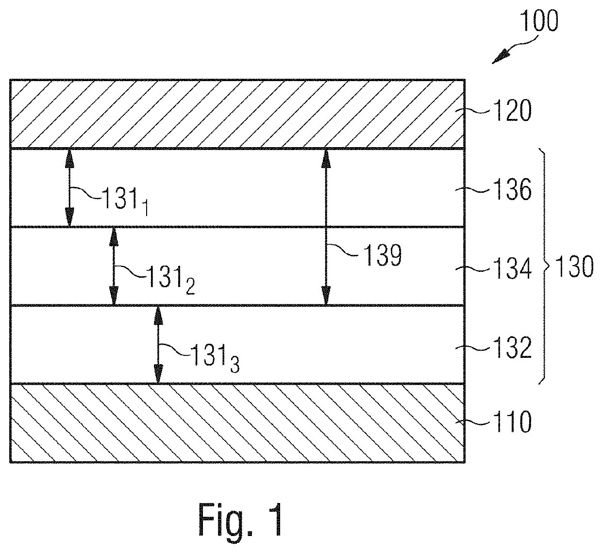
[0057]FIG. 1 shows an embodiment of an integrated capacitor 100 comprising a first electrode structure 110 and a second electrode structure 120. In addition, the integrated capacitor 100 comprises a dielectric layer structure 130 arranged between the first electrode structure 110 and the second electrode structure 120. The dielectric layer structure 130 comprises a layer combination having an SiO2 layer 132, an Si3N4 layer 134, and an SixNy layer 136. The SixNy layer 136 comprises a non-stoichiometric silicon nitride material havin...


PUM

PropertyMeasurementUnit
thicknessaaaaaaaaaa
thicknessaaaaaaaaaa
thicknessaaaaaaaaaa

Abstract

Integrated capacitor including a first electrode structure, a second electrode structure, and an interposed dielectric layer structure. The dielectric layer structure includes a layer combination having an SiO2 layer, an Si3N4 layer, and an SixNy layer. The SixNy layer includes a non-stoichiometric silicon nitride material with an increased proportion of silicon.

Description

CROSS-REFERENCES TO RELATED APPLICATIONS[0001]This application is a continuation of copending International Application No. PCT / EP2019 / 077253, filed Oct. 8, 2019, which is incorporated herein by reference in its entirety, and additionally claims priority from German Applications Nos. DE 102018217249.8, filed Oct. 9, 2018, and DE 102019204503.0, filed Mar. 29, 2019, both of which are incorporated herein by reference in their entirety.[0002]Embodiments in accordance with the invention relate to an integrated capacitor and to a method of producing an integrated capacitor.BACKGROUND OF THE INVENTION[0003]There are various concepts of reducing substrate distortion in manufacturing an integrated capacitor.[0004]A known concept of reducing distortion of semiconductor wafers due to the asymmetry of the mechanical tension between the front and rear sides provides a compensation structure on the rear side of the wafer [1]. However, no concepts—that would be suitable in terms of manufacturing—...

Claims


Application Information

Patent Timeline
Patent Type & Authority Applications(United States)
IPC IPC(8): H01L29/94H01L29/51H01L29/66
CPCH01L29/945H01L29/518H01L29/66181H01L29/511H01G4/40H01L28/40
Inventor BÖTTCHER, NORMANERLBACHER, TOBIAS
Owner FRAUNHOFER GESELLSCHAFT ZUR FOERDERUNG DER ANGEWANDTEN FORSCHUNG EV
Why Eureka
Try Eureka