Buffer circuit and buffer

Active Publication Date: 2021-09-09
CETC CHIPS TECH GRP CO LTD
View PDF0 Cites 0 Cited by
  • Summary
  • Abstract
  • Description
  • Claims
  • Application Information

AI Technical Summary

Benefits of technology

The patent provides a solution for issues such as low linearity, high power consumption, and non-configurable output signal amplitude and bandwidth. It introduces a buffer circuit and buffer technology to address these issues and achieve improved performance.

Problems solved by technology

In the design of analog-to-digital converters, as the sampling speed continues to increase, the kick back effect of the sampling capacitor on the signal source becomes more significant, resulting in a decrease in the sampling linearity of the A / D (analog to digital) converter.
However, although the traditional input buffer increases the isolation, its non-linearity will cause the linearity of the entire A / D converter to decrease.
(1) The power consumption is high. The increase in power consumption does not improve linearity significantly. The multiple of increased linearity is proportional to power consumption. For example, the increase of 6 dB linearity requires 2 times power consumption, and the increase of 12 dB linearity requires 4 times power consumption.
(2) Channel modulation leads to serious nonlinearity. M11 drain-source voltage changes with Vin. For MOS devices in advanced technology, the channel is very short, so the channel modulation effect is more serious, which further leads to a decrease in linearity.
(3) The bandwidth is unadjustable. Since all devices have a fixed size, the output impedance of the buffer is not adjustable, making the bandwidth of the sampling network unadjustable and the application range not wide.

Method used


Image

  • Buffer circuit and buffer
  • Buffer circuit and buffer
  • Buffer circuit and buffer

Examples


Embodiment Construction

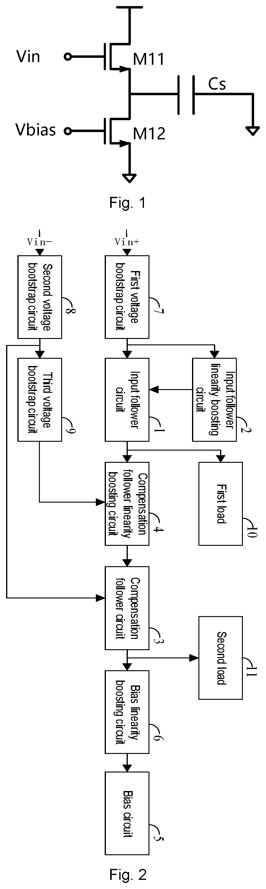
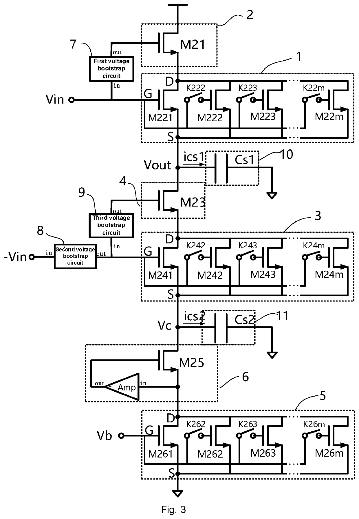
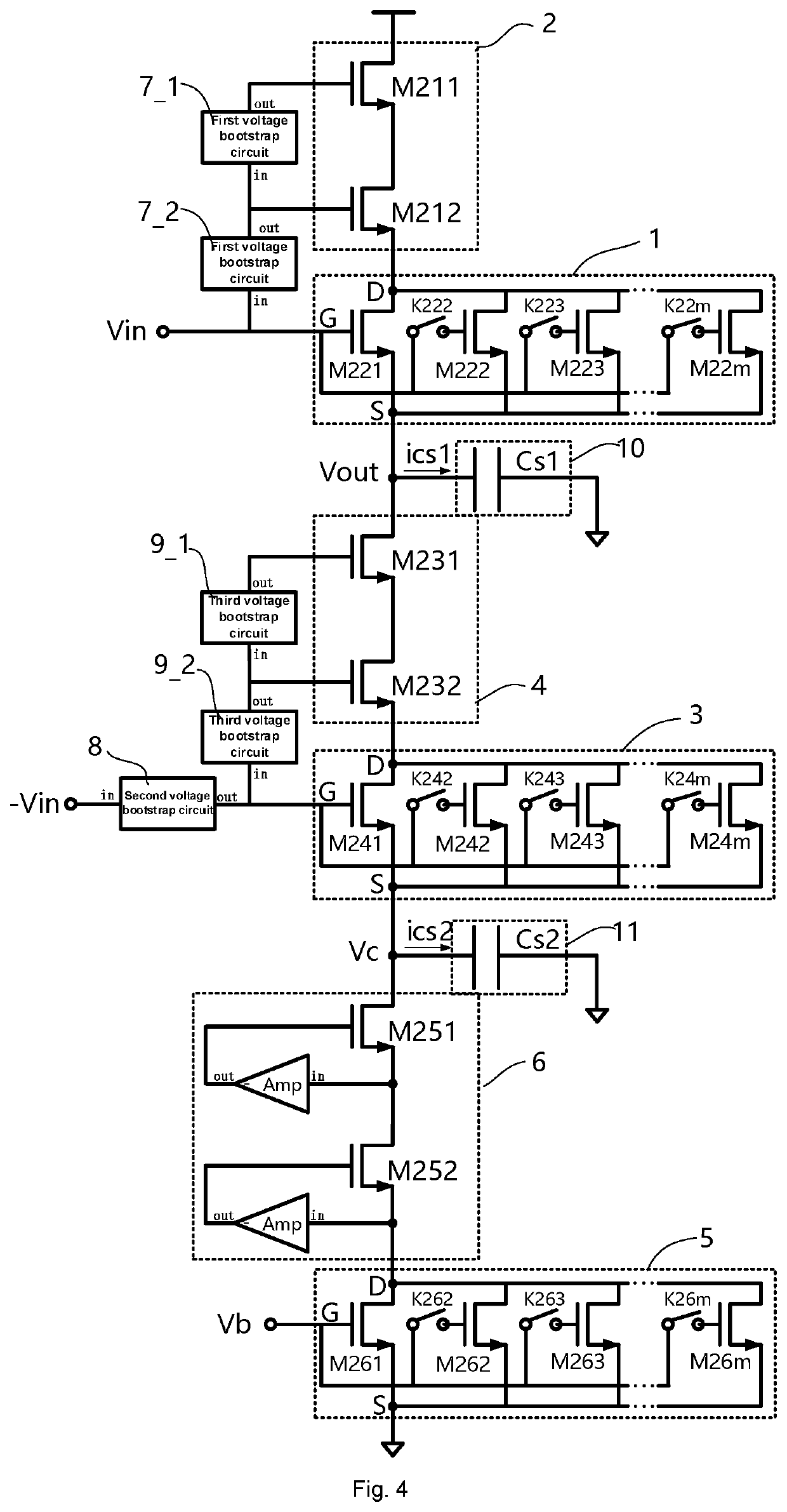
[0046]The embodiments of the present disclosure will be described below through exemplary embodiments. Those skilled in the art can easily understand other advantages and effects of the present disclosure according to contents disclosed by the specification. The present disclosure can also be implemented or applied through other different exemplary embodiments. Various modifications or changes can also be made to all details in the specification based on different points of view and applications without departing from the spirit of the present disclosure. It needs to be stated that the following embodiments and the features in the embodiments can be combined under the situation of no conflict.

[0047]It needs to be stated that the drawings provided in the following embodiments are just used for schematically describing the basic concept of the present disclosure, thus only illustrating components only related to the present disclosure and are not drawn according to the numbers, shapes...


PUM


Abstract

The present disclosure provides a buffer circuit and a buffer. The buffer circuit includes: an input follower circuit for following the voltage change of the first input signal; an input follower linearity boosting circuit for improving follower linearity of the input follower circuit; a first voltage bootstrap circuit for bootstrapping the voltage of the first input signal; a second voltage bootstrap circuit for bootstrapping the voltage of the second input signal; a third voltage bootstrap circuit for providing corresponding quiescent operation point voltage; a compensation follower circuit for following the compensation voltage; a compensation follower linearity boosting circuit for improving follower linearity of the compensation follower circuit; a first load for collecting the buffered voltage; a bias circuit for providing a bias current for the buffer; a bias linearity boosting circuit for improving linearity of the bias circuit; a second load for generating a nonlinear compensation current.

Description

CROSS REFERENCE TO RELATED APPLICATION[0001]This is a Sect. 371 National Stage of PCT International Application No. PCT / CN2018 / 120786, filed on 13 Dec. 2018, which claims priority of a Chinese Patent Application No. 2018109790691 filed on 27 Aug. 2018, the contents of which are incorporated herein by reference in its entirety for all purposes.BACKGROUNDField of Disclosure[0002]The present disclosure relates to the field of integrated circuits, in particular, to a highly linear input buffer circuit and a buffer, which are directly applied to an analog or mixed signal circuit for buffering an input signal, and are particularly suitable for a highly linear analog-to-digital converter.Description of Related Arts[0003]In the design of analog-to-digital converters, as the sampling speed continues to increase, the kick back effect of the sampling capacitor on the signal source becomes more significant, resulting in a decrease in the sampling linearity of the A / D (analog to digital) convert...

Claims


Application Information

Patent Timeline
IPC IPC(8): H03M1/06H03K5/02H03K17/687
CPCH03M1/06H03K17/6871H03K5/02H03M1/0607H03M1/124H03M1/0863
Inventor LI, TINGHU, GANGYILI, RUZHANGZHANG, YONGHUANG, ZHENGBONI, YABOHUANG, XINGFAWANG, JIAN'ANCHEN, GUANGBINGFU, DONGBINGYUAN, JUNXU, ZICHENG
Owner CETC CHIPS TECH GRP CO LTD
Why Eureka
Try Eureka