

Photoresist patterning process
- Summary
- Abstract
- Description
- Claims
- Application Information
AI Technical Summary
Benefits of technology
Problems solved by technology
Method used
Image

Examples
Embodiment Construction
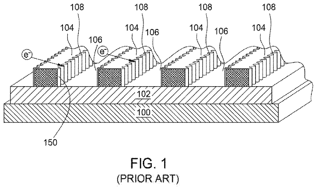
[0020]Methods for enhancing profile control of a photoresist layer formed by photolithography are provided. The diffusion of one or more of ions, electrons, charged particles and acid, generically referred to as drift species, generated by a photoacid generator during pre-exposure and / or a post-exposure bake procedure may be drifted to the nearby or underlying materials or layers so as to assist efficiently transferring features into a target layer. Electric field application controls the diffusion and distribution of the acids and / or other drift species generated by the photoacid generator in the photoresist layer, thus, efficiently altering the film properties to the nearby layers. The altered film properties of the nearby layers may serve as a hardmask layer to assist transferring features into the desired target layer. Suitable process parameters controlled during the pre- and / or post-exposure bake process for the electric field generation includes voltage level as well as the s...
PUM
 Abstract
Description
Claims
Application Information