Copper wire bond on gold bump on semiconductor die bond pad

a technology of copper wire bonding and gold bump, which is applied in the direction of semiconductor devices, semiconductor/solid-state device details, electrical apparatus, etc., can solve the problems of high hardness and brittleness of copper, damage to bond pads and underlying circuits of semiconductor dies, etc., to achieve higher hardness and brittleness, increase and improve the hardness and brittleness

Active Publication Date: 2021-10-07
TEXAS INSTR INC
View PDF0 Cites 0 Cited by
  • Summary
  • Abstract
  • Description
  • Claims
  • Application Information

AI Technical Summary

Benefits of technology

[0007]Copper wire bonds provide advantages in cost and performance over gold wire bonds. For example, copper has higher electrical and thermal conductivity compared to gold. However, copper also has a higher hardness and brittleness compared to gold, and manufacturing techniques for copper wire bonds can damage bond pads and underlying circuity of a semiconductor die in some applications. For this reason, gold bond wires remain preferable in applications where copper wire bonding techniques may cause damage to the semiconductor die or where copper wire bonds may crack.

Problems solved by technology

However, copper also has a higher hardness and brittleness compared to gold, and manufacturing techniques for copper wire bonds can damage bond pads and underlying circuity of a semiconductor die in some applications.

Method used


Image

  • Copper wire bond on gold bump on semiconductor die bond pad
  • Copper wire bond on gold bump on semiconductor die bond pad
  • Copper wire bond on gold bump on semiconductor die bond pad

Examples


Embodiment Construction

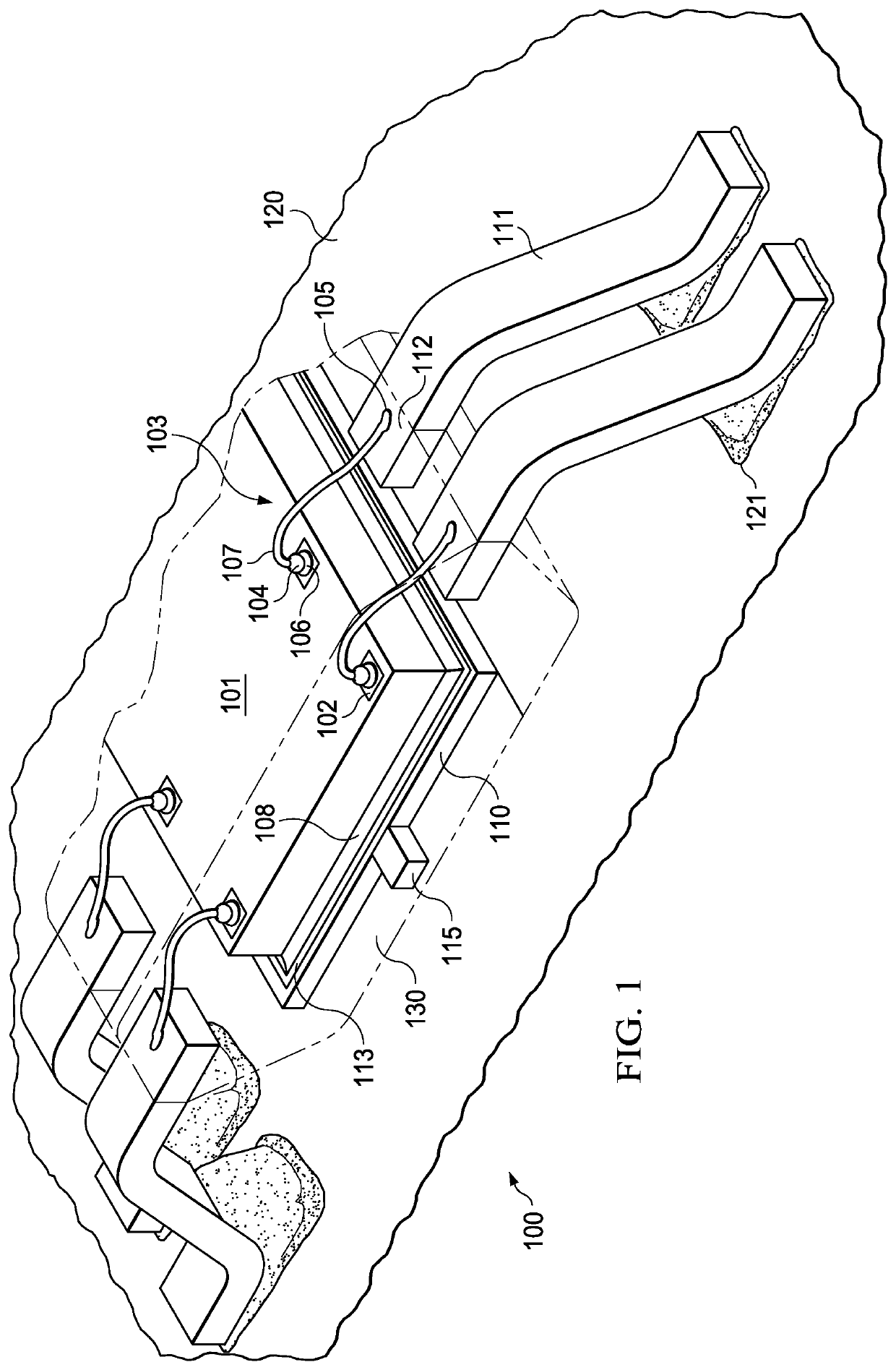
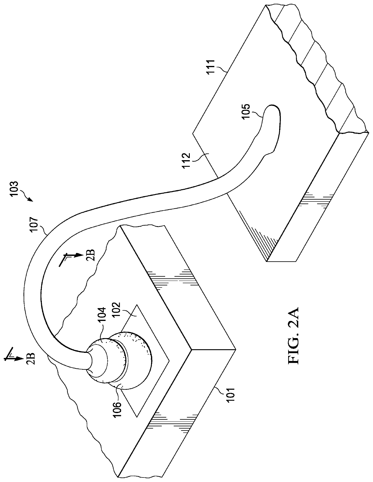
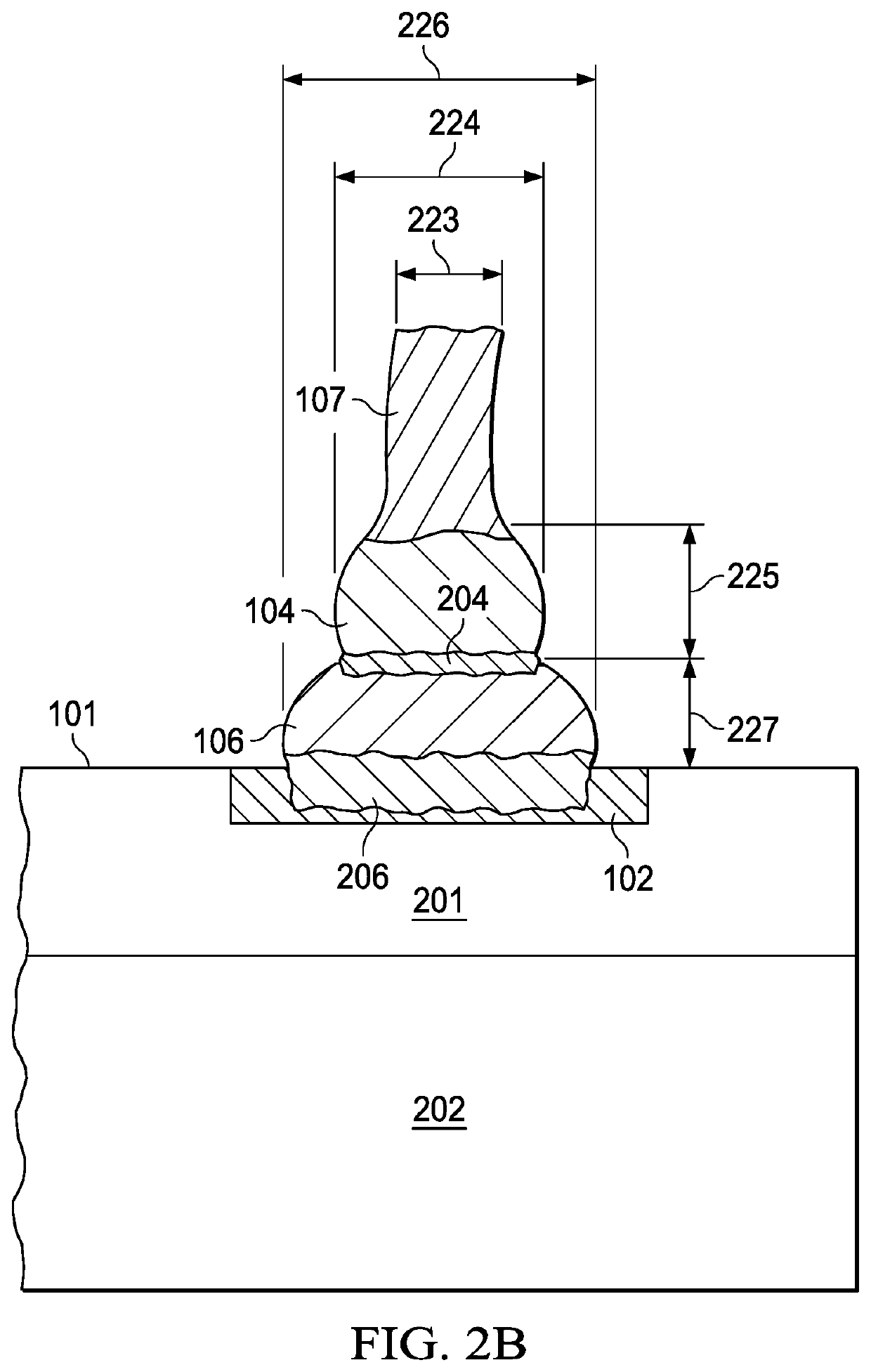
[0017]As disclosed herein, a semiconductor package includes a semiconductor die with a bond pad, a gold bump on the bond pad, and a copper wire bond extending from the gold bump to a conductive pad, such as a stich bonding area of lead. The gold bump may be applied with a lower bond energy than the copper wire bond. During the higher-energy application of the copper wire bond, the gold bump protects the bond pad, mitigating damage to the semiconductor die bond pad and underlying dielectric layers and functional circuity. The disclosed techniques may be utilized in applications where copper wire bonds connected directly to bond pads are not suitable, and provide advantages over gold wire bonds, such as reduced cost, and higher electrical and thermal conductivity. One such example, semiconductor package 100, is illustrated in FIG. 1.

[0018]FIG. 1 is a perspective hidden view of a portion of semiconductor package 100 assembled by solder 121 on a board 120, such as a printed circuit boar...


PUM

PropertyMeasurementUnit
thicknessaaaaaaaaaa
thicknessaaaaaaaaaa
thicknessaaaaaaaaaa

Abstract

A semiconductor package includes a conductive pad, a semiconductor die with an aluminum bond pad over a dielectric layer of the semiconductor die, a gold bump on the aluminum bond pad, a first intermetallic layer of gold and aluminum between the aluminum bond pad and the gold bump, a copper ball bond on the gold bump, a second intermetallic layer of copper and gold between the copper ball bond and the gold bump, a copper wire extending from the copper ball bond to the conductive pad, a stitch bond between the copper wire and the conductive pad.

Description

TECHNICAL FIELD[0001]This disclosure relates to semiconductor packages.BACKGROUND[0002]Semiconductor devices including active and / or passive components may be manufactured into round wafers sliced from elongated cylinder-shaped single crystals of semiconductor elements or compounds. The diameter of these solid-state wafers may reach up to 12 inches or more. Individual semiconductor dies are typically singulated from a round wafer by sawing streets in X- and Y- directions through the wafer in order to create rectangularly shaped discrete pieces from the wafers.[0003]Each semiconductor die includes at least one active or passive component and bond pads serving to facilitate electric connections to the component(s) of the semiconductor die. A bond pad may be a build-up layer of metal, such as aluminum or thick copper with nickel palladium plating, over a metallization layer of a semiconductor die. Semiconductor dies include many large families of functional circuits; examples include a...

Claims


Application Information

Patent Timeline
Patent Type & Authority Applications(United States)
IPC IPC(8): H01L23/00H01L23/498
CPCH01L24/14H01L2224/81205H01L24/46H01L24/11H01L24/43H01L24/73H01L23/49816H01L23/49861H01L24/81H01L2224/05124H01L2224/14505H01L2224/141H01L2224/45147H01L2224/73207H01L2924/01013H01L2924/01029H01L2924/01079H01L24/05H01L23/4952H01L23/3107H01L2224/73265H01L2224/32245H01L2224/48465H01L2224/48247H01L2924/181H01L24/85H01L24/48H01L2224/85205H01L2224/85181H01L2224/05624H01L2224/85207H01L2224/45144H01L2224/85051H01L2224/48499H01L2224/48482H01L24/45H01L2224/05554H01L2924/10161H01L24/32H01L24/78H01L2224/92247H01L2224/83192H01L2224/8385H01L24/83H01L2224/2929H01L24/29H01L2924/00012H01L2924/00014
Inventor ZHANG, LINDUAN, HUO YUNLI, XI LINXIONG, CHENKANG, XIAO LIN
Owner TEXAS INSTR INC
Why Eureka
Try Eureka