Coupling microleds to optical communication channels

a technology of optical communication channel and micro-leds, applied in the field of optical communication system, to achieve the effect of low drive power and high density

Pending Publication Date: 2021-10-14
AVICENATECH CORP
View PDF2 Cites 1 Cited by
  • Summary
  • Abstract
  • Description
  • Claims
  • Application Information

AI Technical Summary

Benefits of technology

This patent describes a way to use small LEDs (microLEDs) to connect chips and chipplets optically. These microLEDs can be very small (some as small as 0.1 μm) and can support high-speed optical communication links with low power consumption. The patent also explains how to efficiently couple these microLEDs to optical communication channels, such as waveguides or free-space. The technical effect of this patent is to provide a practical and efficient way to connect optically integrated circuit chips.

Problems solved by technology

One of the key challenges in usefully applying microLEDs to optical communications is coupling the microLEDs with high efficiency to optical communication channels, whether that communication channel comprises, or in some embodiments consists of, waveguides, free-space, or some combination of the two.

Method used


Image

  • Coupling microleds to optical communication channels
  • Coupling microleds to optical communication channels
  • Coupling microleds to optical communication channels

Examples


Embodiment Construction

0]A microLED is made from a p-n junction of a direct-bandgap semiconductor material. A microLED is distinguished from a semiconductor laser (SL) in the following ways: (1) a microLED does not have an optical resonator structure; (2) the optical output from a microLED is almost completely spontaneous emission whereas the output from a SL is dominantly stimulated emission; (3) the optical output from a microLED is temporally and spatially incoherent whereas the output from a SL has significant temporal and spatial coherence; (4) a microLED is usually designed to be operated down to a zero minimum current, whereas a SL is designed to be operated above a minimum threshold current, which is typically at least 1 mA.

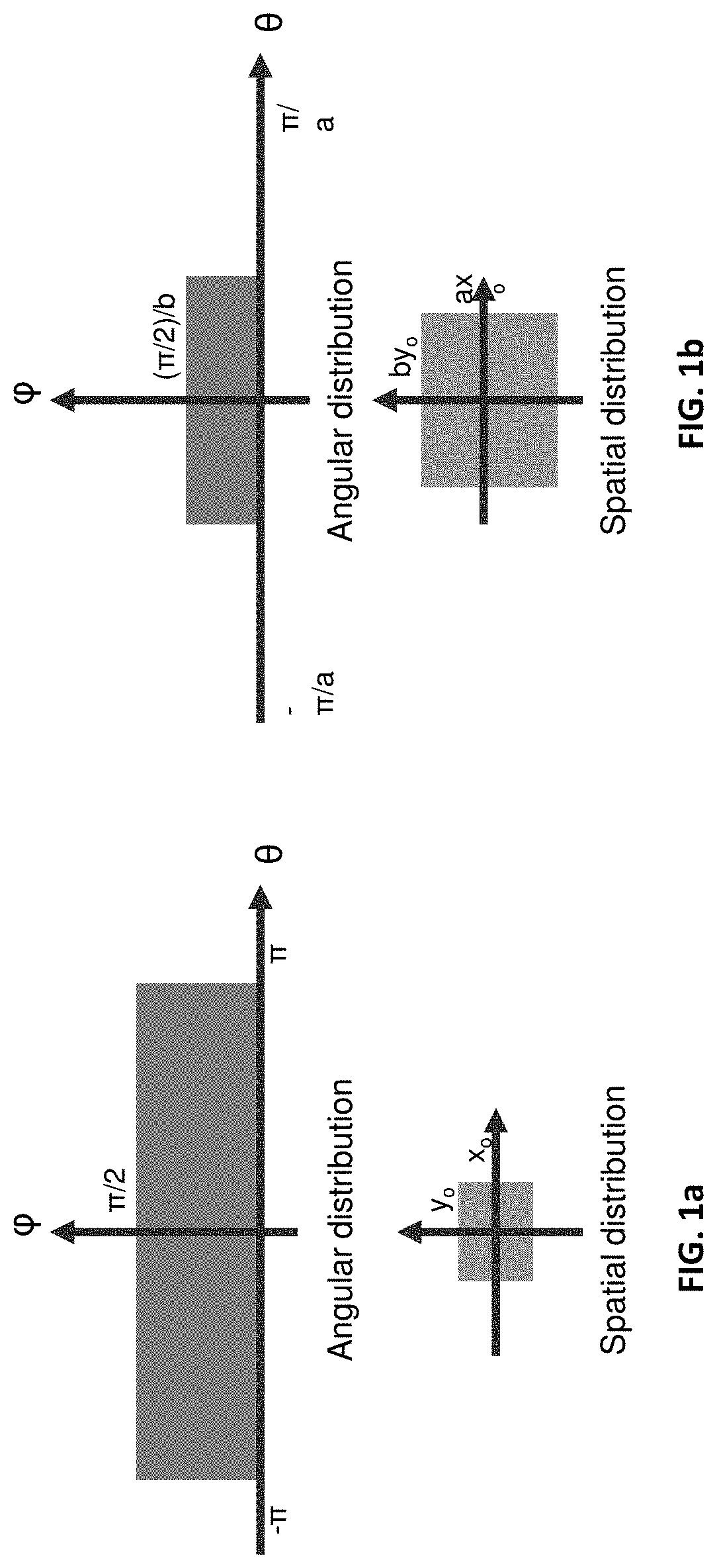
[0051]A microLED may be distinguished from a standard LED by having an emitting region of equal to or less than 20 μm×20 μm. MicroLEDs generally have small etendue, allowing them to be efficiently coupled into small waveguides and / or imaged onto small photodetectors. For conven...


PUM


Abstract

Light from one or more microLEDs may be coupled into multiple waveguide cores. Parabolic reflectors, truncated parabolic reflectors, and encapsulants may be used to increase fraction of emitted light coupled into the waveguide cores.

Description

CROSS REFERENCE TO RELATED APPLICATION[0001]This application claims the benefit of the filing date of U.S. Provisional Patent Application No. 63 / 009,106, filed on Apr. 13, 2020, the disclosure of which is incorporated by reference herein.FIELD OF THE INVENTION[0002]The present invention relates generally to optical communication systems, and more particularly to coupling of microLEDs to communication channels in optical communication systems.BACKGROUND OF THE INVENTION[0003]Desires for high-performance computing and networking is ubiquitous and seemingly ever-present. Prominent applications include data center servers, high-performance computing clusters, artificial neural networks, and network switches.[0004]For decades, dramatic integrated circuit (IC) performance and cost improvements were driven by shrinking transistor dimensions combined with increasing die sizes, summarized in the famous Moore's Law. Transistor counts in the billions have allowed consolidation onto a single sy...

Claims


Application Information

Patent Timeline
IPC IPC(8): G02B6/43H01L33/24H01L33/00H01L33/60H04B10/40H01L33/54
CPCG02B6/43H01L33/24H01L33/54H01L33/60H04B10/40H01L33/0045H01L25/167G02B6/02042G02B6/4206G02B6/4298H04B10/803
Inventor KALMAN, ROBERTPEZESHKI, BARDIATSELIKOV, ALEXANDERDANESH, CAMERON
Owner AVICENATECH CORP
Why Eureka
Try Eureka