Methods of forming structures including silicon germanium and silicon layers, devices formed using the methods, and systems for performing the methods

a technology of silicon germanium and silicon layers, applied in the direction of nanoinformatics, crystal growth process, polycrystalline material growth, etc., can solve the problem of undetected formation of interfacial or interface layer, and achieve the effect of reducing performance variability and improving performan

Pending Publication Date: 2021-10-21
ASM IP HLDG BV
View PDF4 Cites 129 Cited by
  • Summary
  • Abstract
  • Description
  • Claims
  • Application Information

AI Technical Summary

Benefits of technology

[0008]Various embodiments of the present disclosure relate to methods of forming structures, to structures and devices formed using such methods, and to apparatus for performing the methods and / or for forming the structures and / or devices. While the ways in which various embodiments of the disclosure address drawbacks of prior methods and structures are discussed in more detail below, in general, exemplary methods include techniques for forming a relatively thin and abrupt transition layer, which allows for formation of device structures with improved performance and / or devices with reduced performance variability.

Problems solved by technology

Unfortunately, Ge on the surface of the SiGe layer is energetically more favorable than Si on the surface.
Consequently, if the surface of the SiGe layer is not passivated prior to the subsequent Si layer growth, the Ge segregates, resulting in formation of an undesirably large interfacial or interface layer.

Method used


Image

  • Methods of forming structures including silicon germanium and silicon layers, devices formed using the methods, and systems for performing the methods
  • Methods of forming structures including silicon germanium and silicon layers, devices formed using the methods, and systems for performing the methods
  • Methods of forming structures including silicon germanium and silicon layers, devices formed using the methods, and systems for performing the methods

Examples


Embodiment Construction

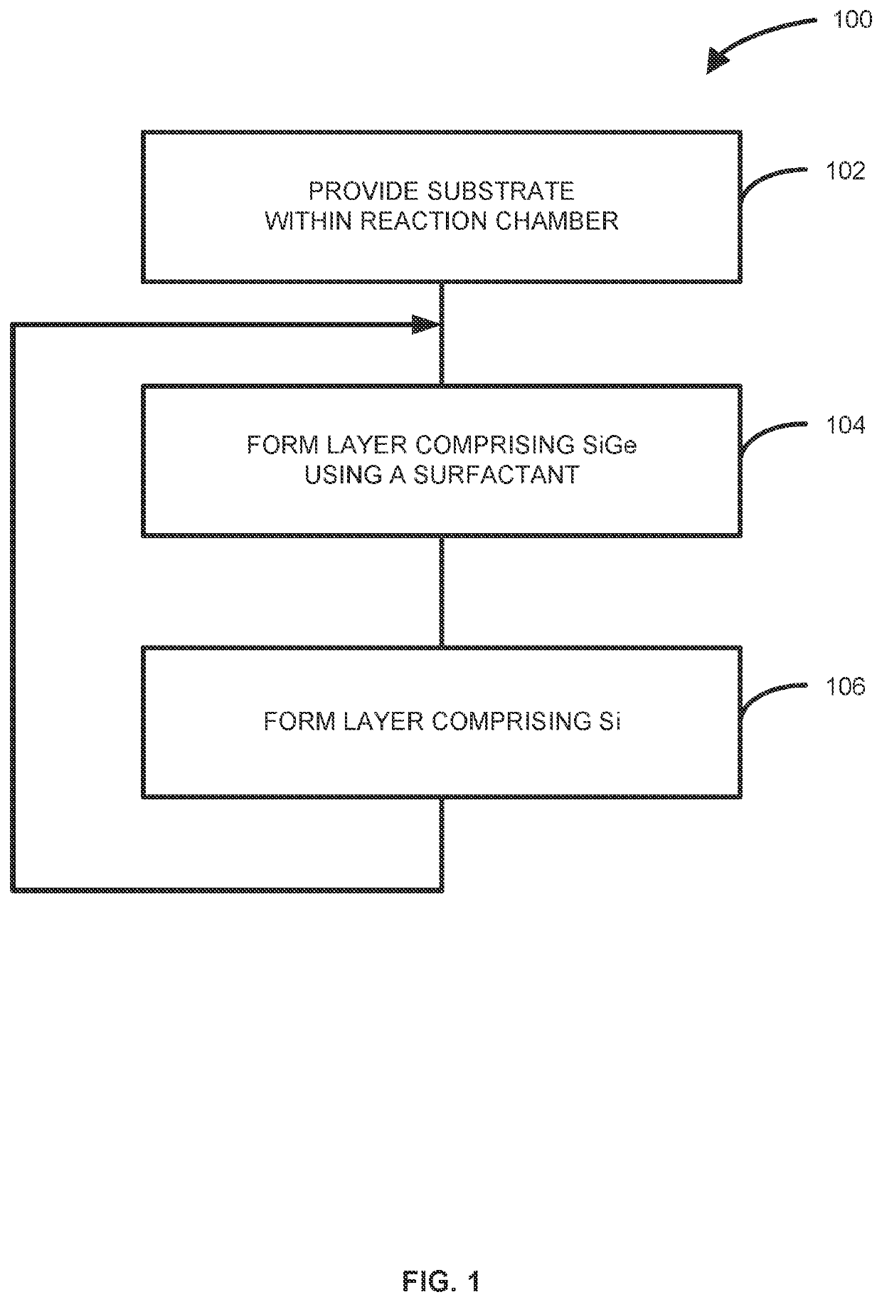
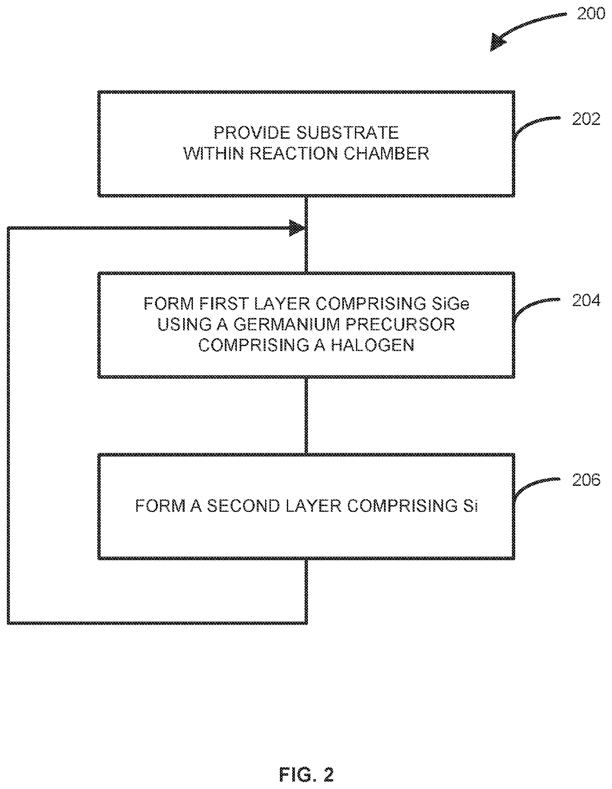
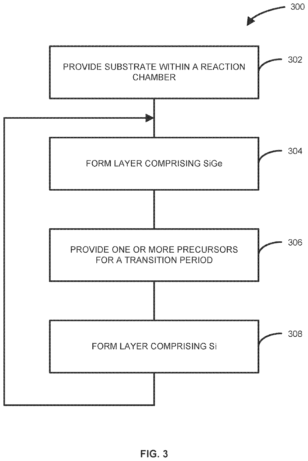
[0023]The description of exemplary embodiments of methods, structures, and reactor systems provided below is merely exemplary and is intended for purposes of illustration only; the following description is not intended to limit the scope of the disclosure or the claims. Moreover, recitation of multiple embodiments having stated features is not intended to exclude other embodiments having additional features or other embodiments incorporating different combinations of the stated features. For example, various embodiments are set forth as exemplary embodiments and may be recited in the dependent claims. Unless otherwise noted, the exemplary embodiments or components thereof may be combined or may be applied separate from each other.

[0024]As set forth in more detail below, various embodiments of the disclosure provide methods for forming structures suitable for forming electronic devices. Exemplary methods can be used to, for example, form structures including one or more layers compri...


PUM

PropertyMeasurementUnit
temperatureaaaaaaaaaa

Abstract

Methods and systems for forming structures including one or more layers comprising silicon germanium and one or more layers comprising silicon are disclosed. Exemplary methods can include using a surfactant, using particular precursors, and / or using a transition step to improve an interface between adjacent layers comprising silicon germanium and comprising silicon.

Description

CROSS-REFERENCE TO RELATED APPLICATIONS[0001]This application is a non-provisional of, and claims priority to and the benefit of, U.S. Provisional Patent Application No. 63 / 011,215, filed Apr. 16, 2020 and entitled, “METHODS OF FORMING STRUCTURES INCLUDING SILICON GERMANIUM AND SILICON LAYERS, DEVICES FORMED USING THE METHODS, AND SYSTEMS FOR PERFORMING THE METHODS,” which is hereby incorporated by reference herein.FIELD OF THE INVENTION[0002]The present disclosure generally relates to methods suitable for forming electronic device structures, to systems for performing the methods, and to structures formed using the methods. More particularly, the disclosure relates to methods and systems for forming structures that include silicon layers and silicon germanium layers.BACKGROUND OF THE DISCLOSURE[0003]Recently, three-dimensional devices, such as gate-all-around (GAA) or nanowire devices, have been developed in an effort to form high-performance devices with increased device density, ...

Claims


Application Information

Patent Timeline
Patent Type & Authority Applications(United States)
IPC IPC(8): H01L21/02C23C16/24C23C16/08C30B25/18C30B29/06C30B29/52C23C16/52
CPCH01L21/0262H01L21/02532H01L21/02603C23C16/24H01L29/0673C30B25/18C30B29/06C30B29/52C23C16/52C23C16/08C30B25/165C30B29/68C23C16/42C23C16/45523H01L21/0245H01L21/02576H01L21/02579H01L21/02507H01L29/66439H01L29/775B82Y10/00B82Y40/00H01L29/42392H01L29/78696C30B25/14
Inventor KAJBAFVALA, AMIRMARGETIS, JOESUN, XINKOHEN, DAVIDPIERREUX, DIETER
Owner ASM IP HLDG BV
Why Eureka
Try Eureka