Power transistor module and controlling method thereof

a technology of power transistor and control method, which is applied in the direction of electronic switching, pulse technique, semiconductor devices, etc., can solve the problems of gate voltage affecting turn-on and turn-off switching time, gate voltage drift of electric characteristics, and loss of switching, so as to reduce the on-resistance (rds,on), the gate voltage can be higher, and the conduction loss of the power transistor device can be reduced.

Active Publication Date: 2021-11-25
FAST SIC SEMICON INC
View PDF0 Cites 0 Cited by
  • Summary
  • Abstract
  • Description
  • Claims
  • Application Information

AI Technical Summary

Benefits of technology

[0015]Based on the above description, in one embodiment of the present disclosure, when the output power of the power transistor module is high, a higher gate voltage can be applied to the power transistor device to reduce the on-resistance (Rds,on) of the power transistor device, whereby the conduction loss of the power transistor device can be reduced, and the efficiency of the power transistor module can be improved. Alternatively, when the output power of the power transistor module is low, a lower gate voltage can be applied to the power transistor device to reduce the electric field applied to the gate insulating layer of the power transistor device, whereby the lifetime of the power transistor device can be increased, and the power consumption required for driving the power transistor device can be reduced.

Problems solved by technology

However, applying a higher gate voltage or high current density to the power transistor may induce the broken of chemical bond at the interface between the gate electrode and the gate dielectric and result in interface defects such as dangling bonds and fixed charges, which may cause the drift of electric characteristics.
In addition to that, a higher gate voltage also increase the electric field exerting on the gate dielectric layer, which adversely impact the lifetime and of gate dielectric layer because the lifetime of gate dielectric layer is inversely proportional to the applied electric field.
In addition to the on-resistance, the gate voltage affects turn-on and turn-off switching time and switching loss.
The switching losses are the power losses due to the overlap of voltage (Vds, drain-to-source voltage in MOSFET) across the device and current (Id, drain current in MOSFET) through the device.
Therefore, for any given Vgs used to turn on or turn off the device, the switching losses (Eon or Eoff) also increase with increasing Id or Vds.
Accordingly, when using a wide band-gap semiconductor power transistor, such as SiC MOSFET, there is a trade-off between lifetime and performance.
Of course people can still increase the active area to obtain a low on-resistance even with a lower gate voltage, however, SiC is an expensive material and increasing the chip area would mean increasing the cost.
Furthermore, the dynamic characteristics of SiC MOSFETs, such as the input capacitance (Ciss), the output capacitance (Coss) and output charge (Qoss) will also increase with increasing chip area, which will result in a higher switching loss and reduce the efficiency.

Method used


Image

  • Power transistor module and controlling method thereof
  • Power transistor module and controlling method thereof
  • Power transistor module and controlling method thereof

Examples


Embodiment Construction

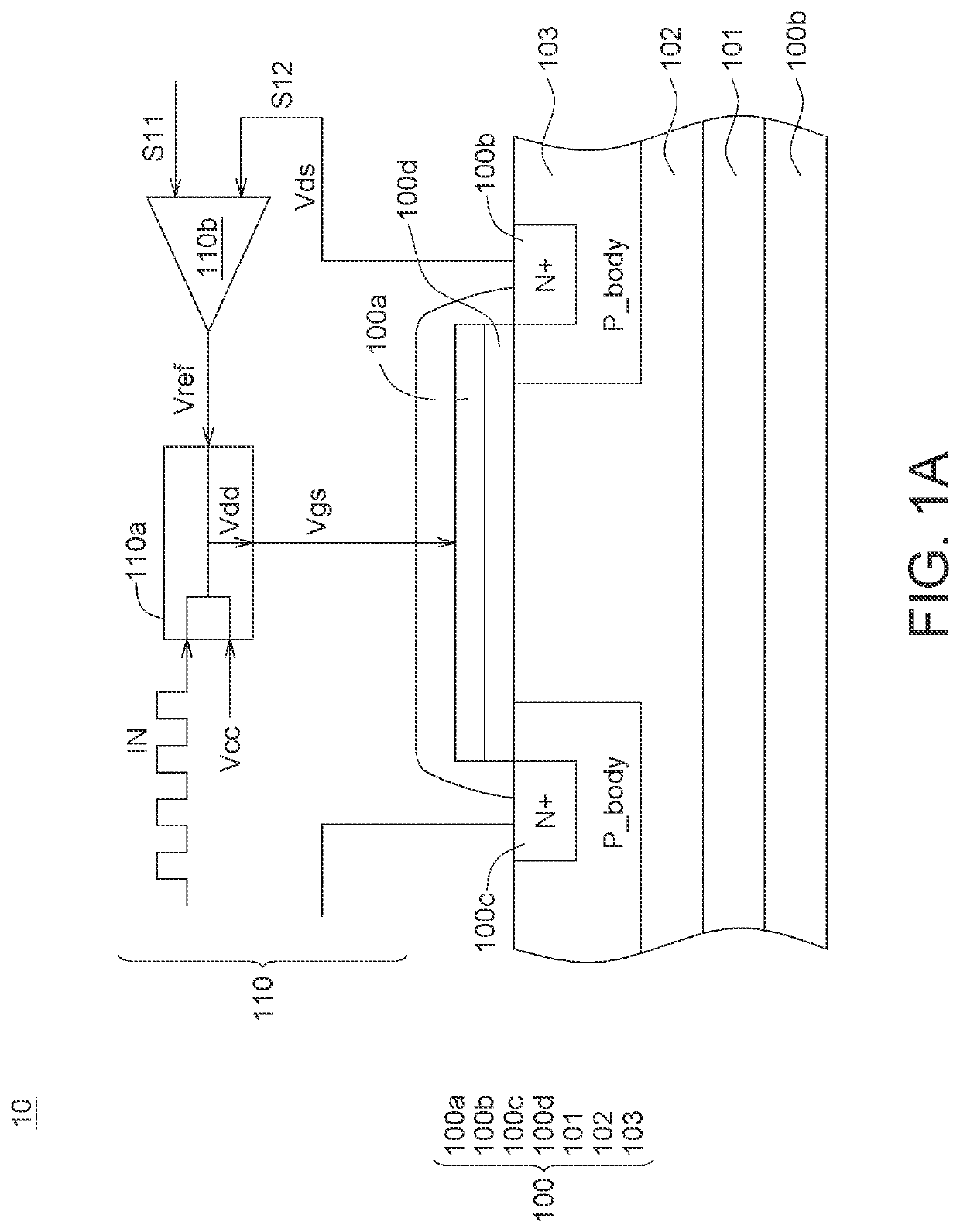
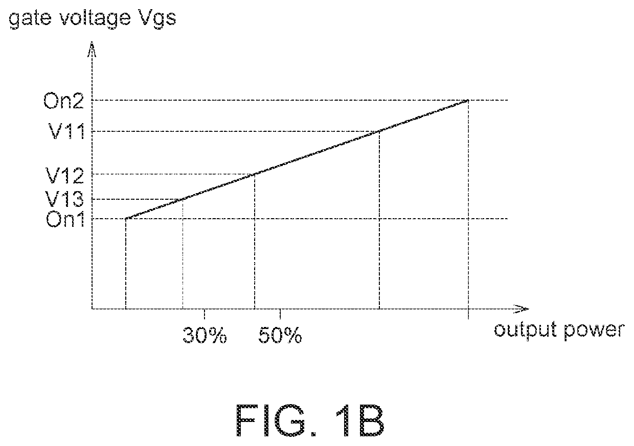
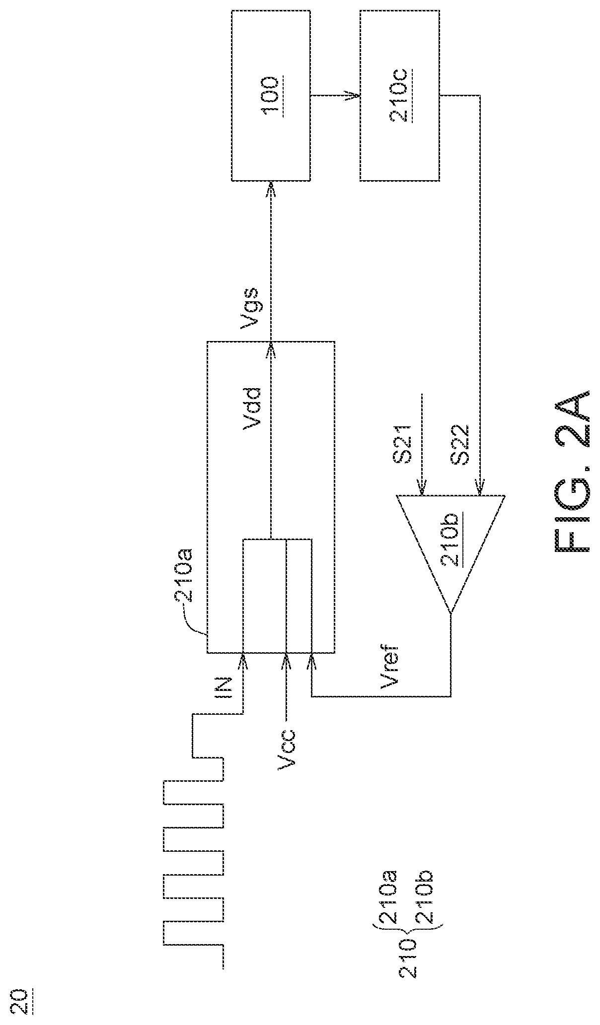
lass="d_n">[0031]The embodiments of the present disclosure provide a power transistor module and the controlling method thereof to reduce the conduction loss and switching loss of the power transistor device built in the power transistor module and extend its lifetime. The present disclosure will now be described more specifically with reference to the following embodiments illustrating the structure and arrangements thereof.

[0032]It should be noted that these embodiments are illustrative and for explanatory purposes only, not for limiting the scope of protection of the invention. The invention can be implemented by using other features, elements, methods and parameters. The preferred embodiments are merely for illustrating the technical features of the disclosure, not for limiting the scope of protection. Anyone skilled in the technology field of the disclosure will be able to make suitable modifications or changes based on the specification disclosed below without breaching the sp...


PUM


Abstract

A power transistor module includes a power transistor device and a control circuit. The control circuit is electrically connected to the power transistor device for providing at least one gate voltage to drive the power transistor device, and adjusting the at least one gate voltage in response to an output power of the power transistor module. When the output power is greater than a predetermined power load, the at least one gate voltage has a first swing amplitude; and when the output power is less than or equal to the predetermined power load the at least one gate voltage has a second swing amplitude less than the first swing amplitude.

Description

[0001]This application is a continuation-in-part (CIP) application of U.S. application Ser. No. 17 / 151,737, filed on Jan. 19, 2021, which claims the benefit of U.S. provisional application Ser. No. 62 / 963,187, filed Jan. 20, 2020, and U.S. provisional application Ser. No. 63 / 093,797, filed Oct. 20, 2020, the subject matters of which are incorporated herein by references.BACKGROUNDTechnical Field[0002]The disclosure relates in general to a power electronic module and the controlling method thereof, and more particularly to a power transistor module and the controlling method thereof.Description of the Related Art[0003]The power system of various electronic devices must undergo several power conversions, such as direct current / alternating current conversion (AC / DC) or direct current / direct current conversion (DC / DC), during the utilization and transmission of electric power. With the increasing demand in electric power and the requirements of saving energy, the power electronic device...

Claims


Application Information

Patent Timeline
Patent Type & Authority Applications(United States)
IPC IPC(8): H03K17/60H03K17/082H03K17/16H03K17/567
CPCH03K17/60H03K17/567H03K17/165H03K17/0826
Inventor YEN, CHENG-TYNGHSU, FU-JENHUNG, HSIANG-TING
Owner FAST SIC SEMICON INC
Why Eureka
Try Eureka