Wafer placement table

Pending Publication Date: 2021-12-23
NGK INSULATORS LTD
View PDF0 Cites 0 Cited by
  • Summary
  • Abstract
  • Description
  • Claims
  • Application Information

AI Technical Summary

Benefits of technology

[0012]In the wafer placement table, the outer peripheral surface of the portion of the power supply terminal, inserted in the hole for power supply terminal is covered with an insulating thin film that is formed by coating of an insulating material. Therefore, the diameter of the hole for power supply terminal provided in the cooling member can be reduced according to the diameter of a portion of the power supply terminal, the portion being covered with an insulating thin film. Although the hole for power supply terminal is a singular section where heat removal of heat input from plasma is not made directly downward, the diameter of the hole for power supply terminal can be reduced, thus the singular section can be decreased, and eventually, the temperature uniformity of the wafer placement surface and the wafer is improved.
[0013]In the wafer placement table of the present invention, the insulating thin film

Problems solved by technology

However, if the ceramic sleeve is thick, the diameter of the hole for power supply terminal to be opened in the cooling memb

Method used


Image

  • Wafer placement table
  • Wafer placement table

Examples


Embodiment Construction

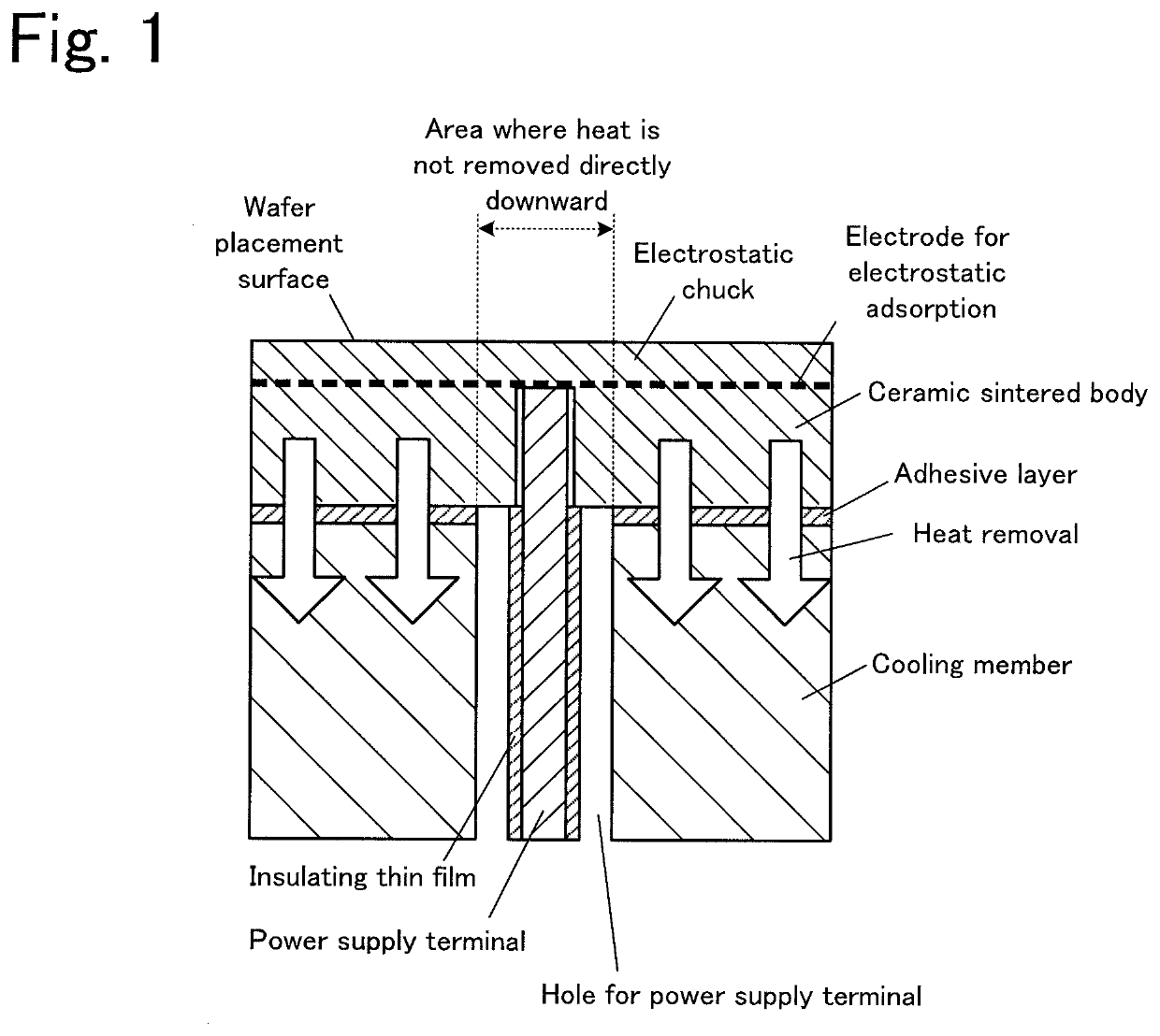
[0018]A preferred embodiment of the present invention will be described below with reference to the drawings. FIG. 1 is a vertical cross-sectional view of a main part of a wafer placement table of the present embodiment.

[0019]As shown in FIG. 1, the wafer placement table includes an electrostatic chuck, a cooling member, a hole for power supply terminal, and a power supply terminal. The electrostatic chuck is a disc-shaped ceramic sintered body in which an electrode for electrostatic adsorption is embedded, and when a voltage is applied to the electrode for electrostatic adsorption, a wafer (not shown) placed on the wafer placement surface of the electrostatic chuck is electrostatically adsorbed by the electrostatic chuck. The cooling member is a metal member having a cooling medium passage (not shown) inside, and cools the electrostatic chuck. The hole for power supply terminal penetrates the cooling member in a thickness direction. The power supply terminal is wax-bonded to the el...


PUM


Abstract

A wafer placement table includes: an electrostatic chuck that is a ceramic sintered body in which an electrode for electrostatic adsorption is embedded; a cooling member which is bonded to a surface on an opposite side of a wafer placement surface of the electrostatic chuck, and cools the electrostatic chuck; a hole for power supply terminal, the hole penetrating the cooling member in a thickness direction; and a power supply terminal which is bonded to the electrode for electrostatic adsorption from the surface on the opposite side of the wafer placement surface of the electrostatic chuck, and is inserted in the hole for power supply terminal. The outer peripheral surface of a portion of the power supply terminal is covered with an insulating thin film that is formed by coating of an insulating material, the portion being inserted in the hole for power supply terminal.

Description

BACKGROUND OF THE INVENTION1. Field of the Invention[0001]The present invention relates to a wafer placement table.2. Description of the Related Art[0002]A wafer placement table that sucks and holds a wafer has been conventionally used in transfer, exposure, a film deposition process such as CVD, washing, etching, and microfabrication such as dicing, for a semiconductor wafer. As shown in PTL 1, such a wafer placement table is known, which includes an electrostatic chuck that is a ceramic sintered body in which an electrode for electrostatic adsorption is embedded; a cooling member that cools the electrostatic chuck; and a power supply terminal which is inserted in a hole for power supply terminal and bonded to the electrode for electrostatic adsorption, the hole penetrating the cooling member in a thickness direction. The electrostatic chuck and the cooling member are bonded via an adhesive layer. The outer periphery of the power supply terminal is surrounded by an insulating mater...

Claims


Application Information

Patent Timeline
IPC IPC(8): H01L21/683
CPCH01L21/6833H02N13/00H01L21/67109H01L21/68785B23Q3/15
Inventor AIKAWA, KENICHIROTAKEBAYASHI, HIROSHIKUNO, TATSUYA
Owner NGK INSULATORS LTD
Why Eureka
Try Eureka