TFT array substrate and manufacturing method thereof

Inactive Publication Date: 2021-12-30
SHENZHEN CHINA STAR OPTOELECTRONICS TECH CO LTD
View PDF0 Cites 0 Cited by
  • Summary
  • Abstract
  • Description
  • Claims
  • Application Information

AI Technical Summary

Benefits of technology

The present invention provides a TFT and a manufacturing method that solves a problem where a prior TFT had long tail fibers in the semiconductor layer that could cause leakage currents when exposed to light. This invention uses a four-mask process to remove the tail fibers and align the edges of the semiconductor layer with the edges of the source and drain. This reduces the photoelectric sensitivity of the TFT and reduces the size of the TFT device, which saves layout space and simplifies processes. Overall, this invention improves display quality and increases the production efficiency of liquid crystal panels.

Problems solved by technology

However, since the semiconductor layer is usually made of a photosensitive material, during an application of a display panel, when refracted light or reflected light irradiates on a part of the exposed semiconductor layer of the TFT device, a leakage current of the TFT device is easily increased, which makes a holding ability of a pixel voltage weak and affects display quality of the display panel.

Method used


Image

  • TFT array substrate and manufacturing method thereof
  • TFT array substrate and manufacturing method thereof
  • TFT array substrate and manufacturing method thereof

Examples


Embodiment Construction

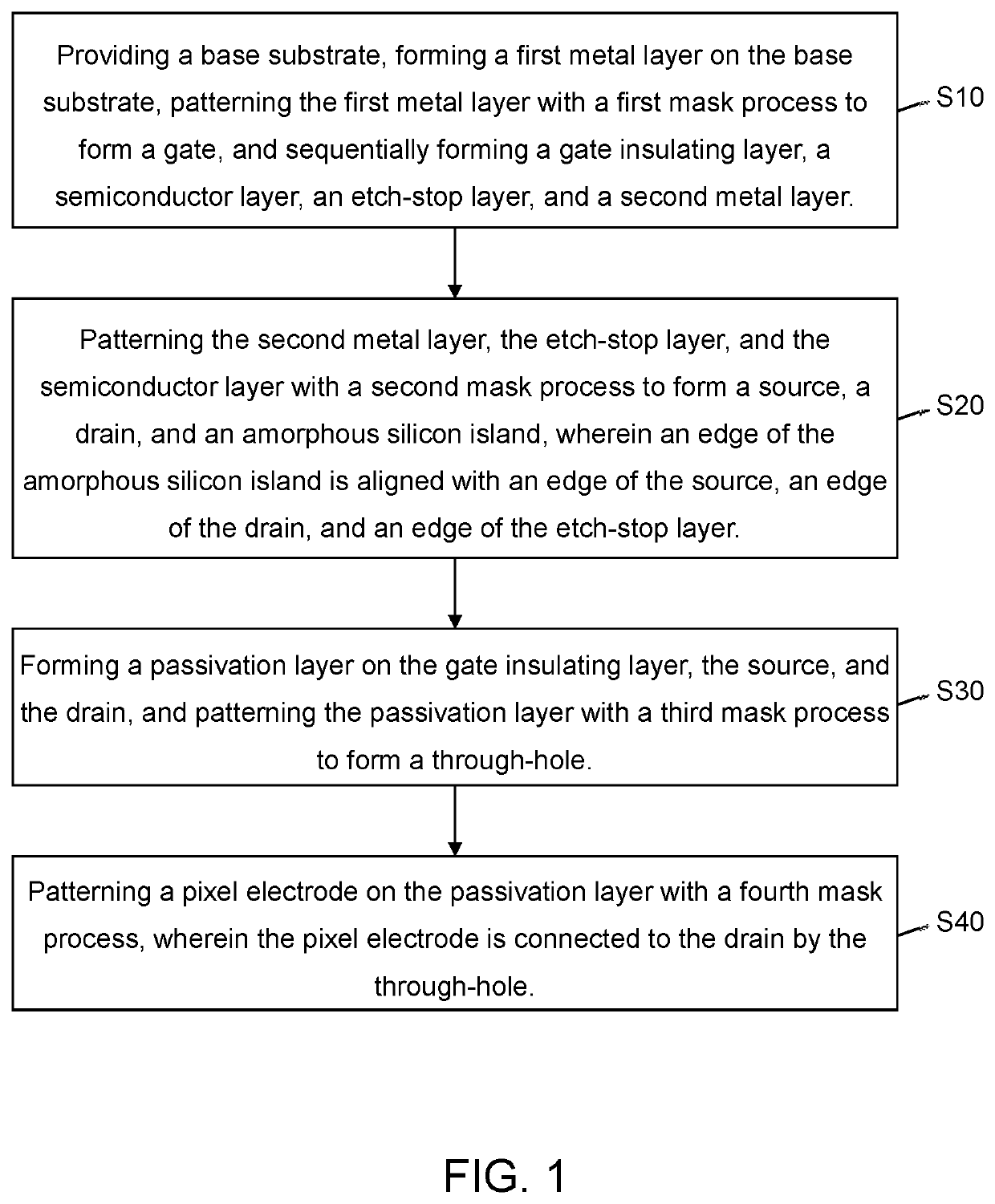
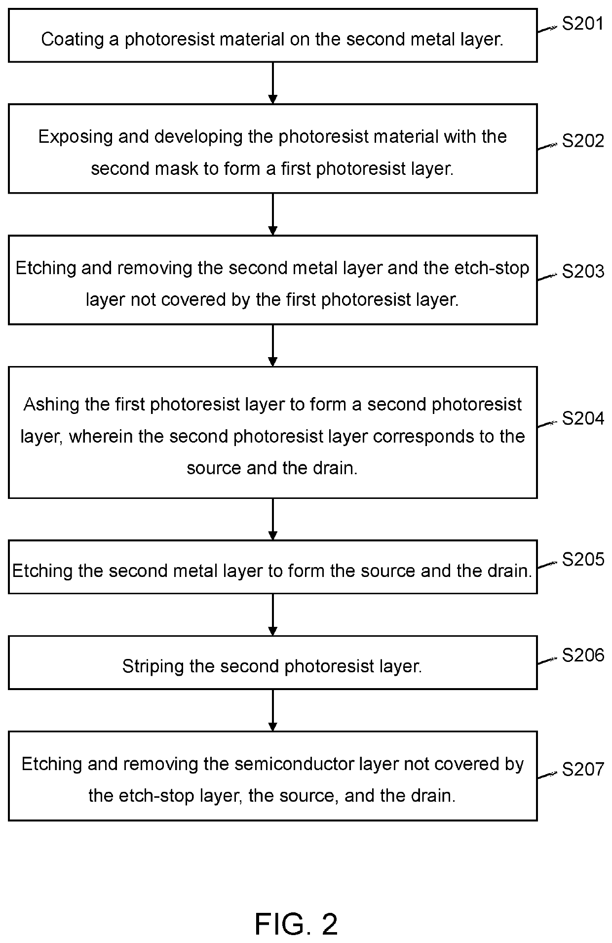
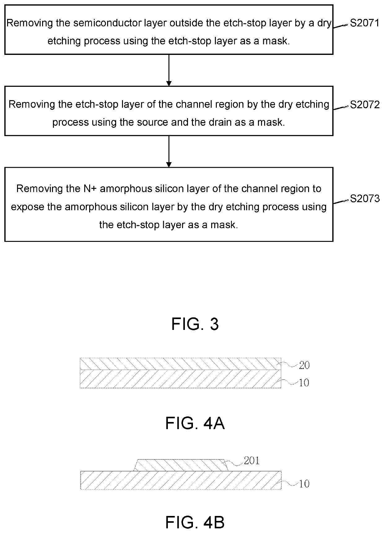
[0071]Examples are described below with reference to the appended drawings, and the drawings illustrate particular embodiments in which the present invention may be practiced. Directional terms mentioned in the present invention, such as upper, lower, front, rear, left, right, in, out, side, etc., only refer to directions in the accompanying drawings. Thus, the adoption of directional terms is used to describe and understand the present invention, but not to limit the present invention. In the drawings, units of similar structures are represented using the same numerals.

[0072]The present invention can solve defects of a thin-film transistor (TFT) array substrate and a manufacturing method thereof of the prior art. Because tail fibers of a certain length exist in a semiconductor layer under a source and a drain, which easily leads a leakage current of a TFT device to increase when refracted light or reflected light irradiates on a part of the exposed semiconductor layer of the TFT de...


PUM


Abstract

The present invention provides a thin-film transistor (TFT) array substrate and a manufacturing method thereof. The manufacturing method uses a four-mask process that uses an etch-stop layer on a semiconductor layer as a mask to perform alignment and etching to form a pattern of an amorphous silicon island. Tail fibers exposed outside of a source and a drain are removed, photoelectric sensitivity of a TFT device can be effectively reduced, and size of the TFT device is reduced, which can simplify processes, save layout space, and effectively increase display quality of large-size and high-resolution liquid crystal panels under high backlight intensity.

Description

FIELD OF INVENTION[0001]The present invention is related to the display field, and specifically to a thin-film transistor (TFT) array substrate and a manufacturing method thereof.BACKGROUND OF INVENTION[0002]With the development of large-size and high-resolution liquid crystal display panels, in order to increase display quality of high-end products, luminous intensity of backlight of liquid crystal display panels is increased, pixel size is decreased, and thin-film transistor (TFT) devices of the liquid crystal display panels accordingly require a higher standard.[0003]The TFT devices are multilayer thin-film structures formed by multiple exposure, development, and etching processes. In a traditional process, a TFT device need to be formed by a four-mask process. In a traditional four-mask process, an amorphous silicon island, a source, and a drain need to be formed by a one-mask process for exposure and development, two wet etchings, and two dry etchings. Due to a difference betwe...

Claims


Application Information

Patent Timeline
IPC IPC(8): H01L27/12H01L29/786
CPCH01L27/127H01L29/78669H01L27/1288H01L27/1214H01L21/77G02F1/1333G02F1/1362G02F1/136227G02F1/136277G02F1/136236H01L29/66765
Inventor LONG, FEN
Owner SHENZHEN CHINA STAR OPTOELECTRONICS TECH CO LTD
Why Eureka
Try Eureka