Laminate, printed wiring board, semiconductor package, and method for manufacturing laminate

a technology of printed wiring boards and laminates, which is applied in the direction of printed circuits, stress/warp reduction, other domestic objects, etc., can solve the problems of warpage, difference in thermal expansion coefficient, and reduction of size and thickness, so as to improve drilling workability, high elastic modulus, and low thermal expansion

Pending Publication Date: 2022-03-17
RESONAC CORP
View PDF0 Cites 2 Cited by
  • Summary
  • Abstract
  • Description
  • Claims
  • Application Information

AI Technical Summary

Benefits of technology

[0042]According to the present invention, a laminate that is excellent in drilling workability while having a high elastic modulus and a low thermal expansion, a printed wiring board using the laminate, a semiconductor package, and a method for producing a laminate can be provided.

Problems solved by technology

In particular, a semiconductor package involves a severe issue of occurrence of warpage in mounting components and fabricating the package, associated with the reduction of the size and the thickness thereof.
One of the factors of the warpage of the semiconductor package is the difference in thermal expansion coefficient between the semiconductor element and the printed wiring board having the semiconductor element mounted thereon.
The thermal expansion coefficient of the printed wiring board is generally larger than the thermal expansion coefficient of the semiconductor element, and therefore the package experiencing a thermal history including heating for mounting the semiconductor element undergoes warpage caused by the difference in thermal expansion coefficient.
However, the inorganic filler highly filled therein leads a concern over deterioration of the insulation reliability, the adhesiveness to a copper foil, the press workability, and the like, and therefore in consideration of the standpoint of the securement of these capabilities, there is a limitation in increasing the elastic modulus and decreasing the thermal expansion of the laminate only by highly filling the inorganic filler.

Method used


Image

  • Laminate, printed wiring board, semiconductor package, and method for manufacturing laminate
  • Laminate, printed wiring board, semiconductor package, and method for manufacturing laminate
  • Laminate, printed wiring board, semiconductor package, and method for manufacturing laminate

Examples


example 1

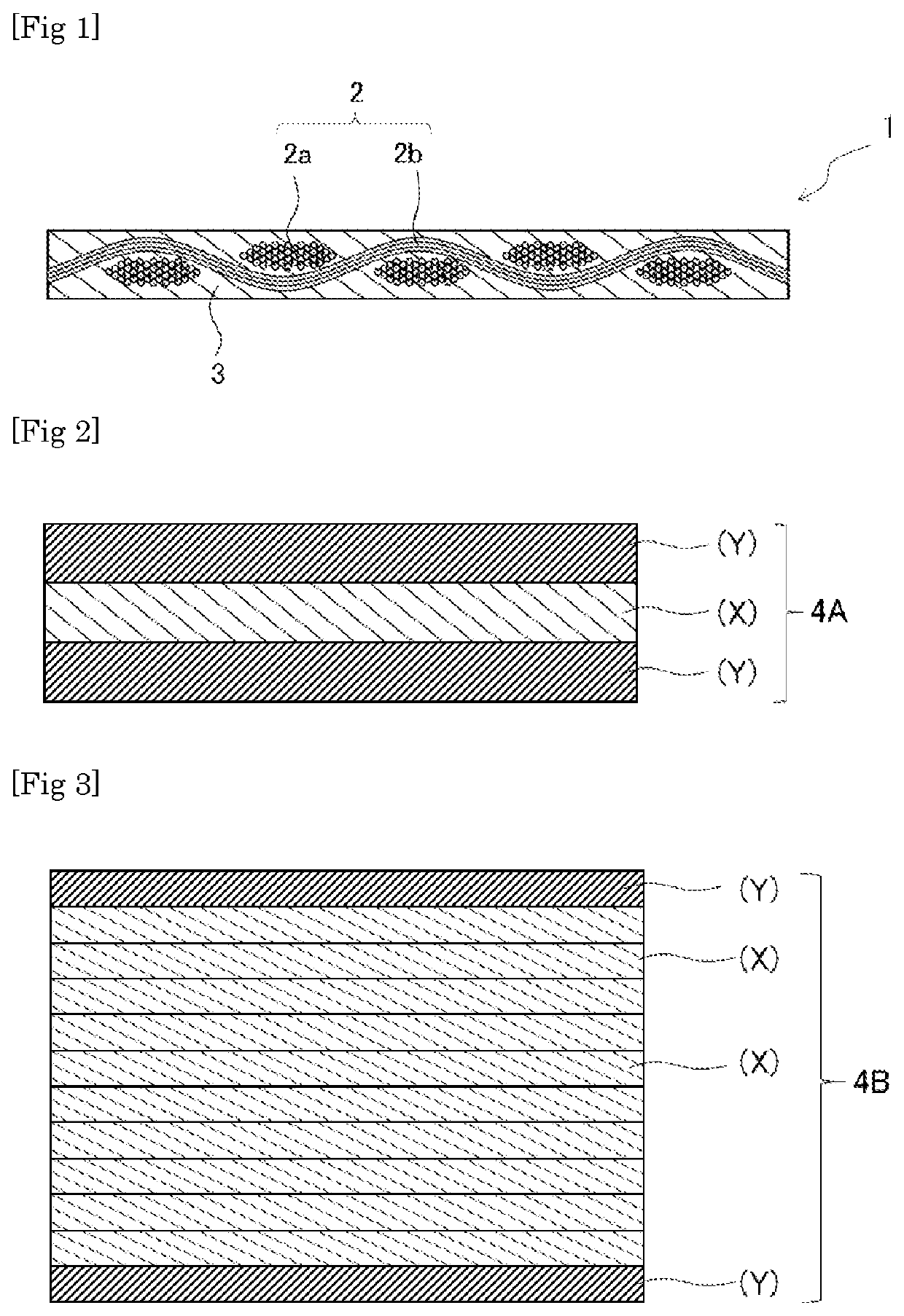
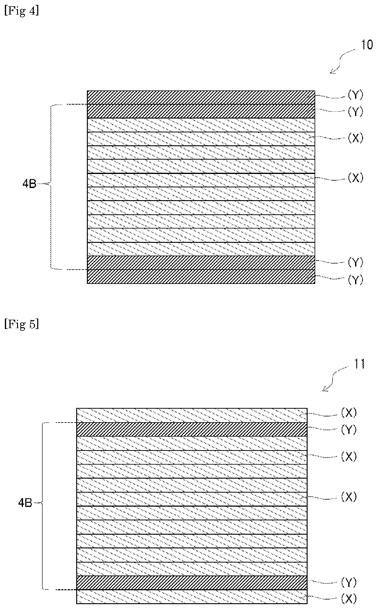
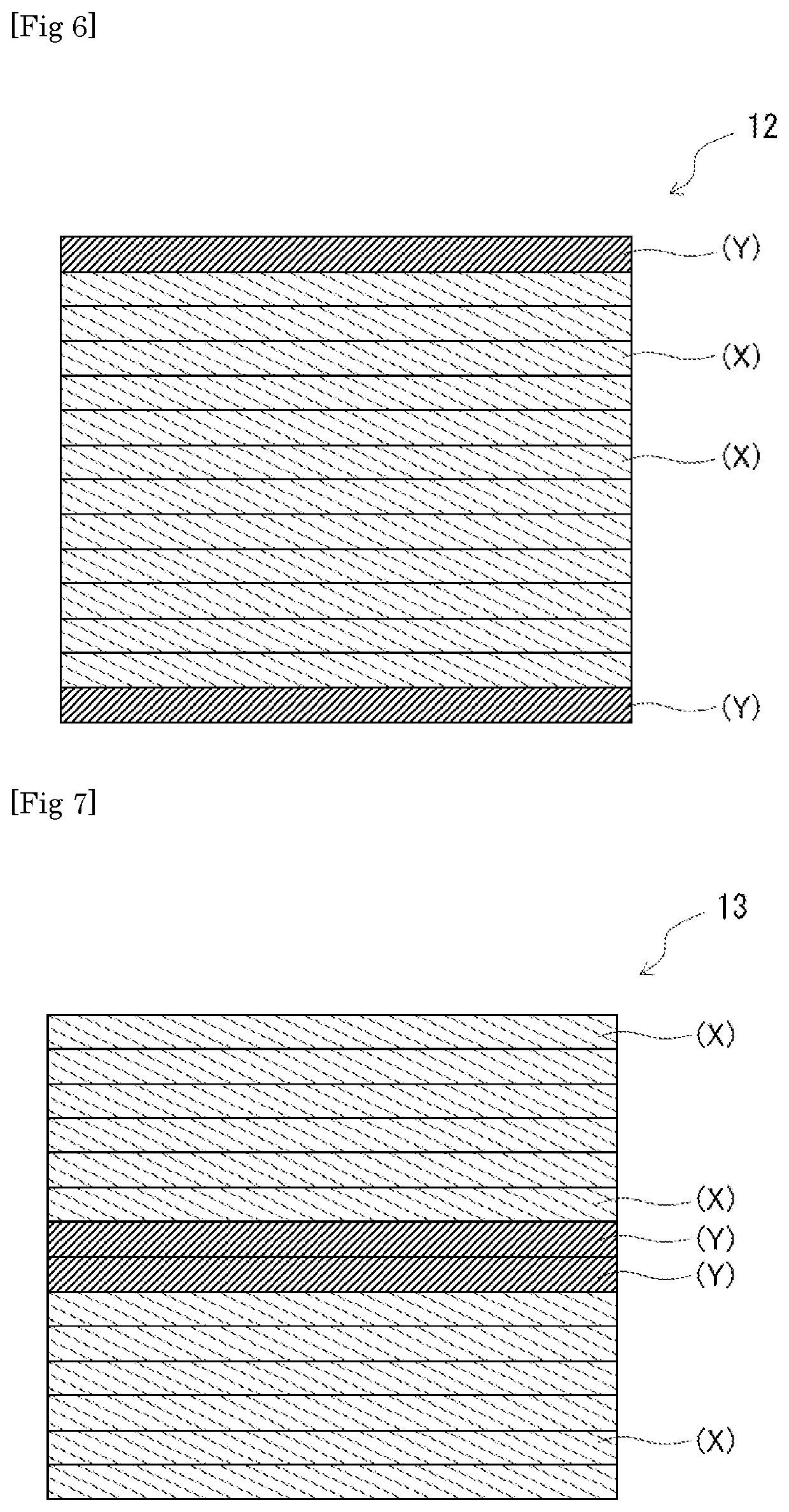
(Copper-Clad Laminate 1: Copper-Clad Laminate Having Copper Foils on Both Surfaces of Laminate Shown in FIG. 6)

(1) Production of Varnish

[0204]In a reaction vessel having a capacity of 1 L capable of being heated and cooled, equipped with a thermometer, an agitation device, and a reflux condenser, 19.4 g of siloxanediamine (X-22-161A, trade name, produced by Dow Corning Toray Co., Ltd., functional group equivalent of amino group: 800 g / mol), 13.0 g of 3,3′-diethyl-4,4′-diaminodiphenylmethane, 122.9 g of N,N-(4,4′-diphenylmethane)bismaleimide, 4.7 g of p-aminophenol, and 240.0 g of propylene glycol monomethyl ether were placed, and reacted at 115° C., and then the reaction mixture was concentrated under ordinary pressure to make a resin concentration of 60% by mass, to which 53.3 g of cyclohexanone was further added at 90° C., followed by agitating for 30 minutes, so as to provide an intermediate varnish.

[0205]303.5 g of the intermediate varnish, 601.0 g of a methyl isobutyl ketone so...

example 2

(Copper-Clad Laminate 2: Copper-Clad Laminate Having Copper Foils on Both Surfaces of Laminate Shown in FIG. 4)

[0208]A copper-clad laminate 2 was obtained in the same manner as in Example 1 except that the lamination structure of the prepregs in Example 1 was changed to 10 layers of the prepregs including the E-glass cloth inside having disposed on each of the outermost layers on both sides thereof two layers of the prepregs including the S-glass cloth.

example 3

(Copper-Clad Laminate 3: Copper-Clad Laminate Having Copper Foils on Both Surfaces of Laminate Shown in FIG. 7)

[0209]A copper-clad laminate 3 was obtained in the same manner as in Example 1 except that the lamination structure of the prepregs in Example 1 was changed to 6 layers of the prepregs including the E-glass cloth, 2 layers of the prepregs including the S-glass cloth, and 6 layers of the prepregs including the E-glass cloth in this order.


PUM

PropertyMeasurementUnit
tensile elastic modulusaaaaaaaaaa
thicknessaaaaaaaaaa
thicknessaaaaaaaaaa

Abstract

The present invention relates to a laminate including two or more layers of a composite layer including a fiber substrate and a cured product of a thermosetting resin composition, the two or more layers of the composite layer including one or more layer of a composite layer (X) and one or more layer of a composite layer (Y), the composite layer (X) being a layer including a first fiber substrate constituted by first glass fibers, the composite layer (Y) being a layer including a second fiber substrate constituted by second glass fibers, and the second glass fibers having a higher tensile elastic modulus at 25° C. than the first glass fibers, a printed wiring board including the laminate, a semiconductor package, and a method for producing a laminate.

Description

TECHNICAL FIELD[0001]The present invention relates to a laminate, a printed wiring board, a semiconductor package, and a method for producing a laminate.BACKGROUND ART[0002]According to the size reduction and the enhancement of capabilities of electronic equipments in recent years, the increase of the wiring density and the integration degree of a printed wiring board proceed, and associated therewith, there has been an increasing demand for enhancing the reliability of the printed wiring board. In particular, a semiconductor package involves a severe issue of occurrence of warpage in mounting components and fabricating the package, associated with the reduction of the size and the thickness thereof.[0003]One of the factors of the warpage of the semiconductor package is the difference in thermal expansion coefficient between the semiconductor element and the printed wiring board having the semiconductor element mounted thereon. The thermal expansion coefficient of the printed wiring...

Claims


Application Information

Patent Timeline
Patent Type & Authority Applications(United States)
IPC IPC(8): B32B5/26H05K1/03B32B5/02B32B15/14B32B17/04B32B15/20B29C70/16
CPCB32B5/263B29K2101/10B32B5/024B32B15/14B32B17/04B32B15/20B29C70/16H05K2201/029B32B2262/101B32B2307/54B32B2457/08B32B2307/732B32B2260/023B32B2260/046H05K1/036B29C70/30B32B7/022B32B5/02B32B5/26B32B2250/05B32B2250/20B32B2250/40B32B2264/104B32B2264/101B32B7/02B32B2264/107B32B2307/206B32B5/022B32B2264/102H05K1/0366H05K1/0271H05K2201/068B29C70/003H01L23/12H05K1/0306H05K1/038B29K2105/0872B32B2305/076B29K2309/08B29L2009/00
Inventor MURAKAMI, NORIAKIUCHIMURA, RYOICHIOSE, MASAHISAOHHASHI, KENICHI
Owner RESONAC CORP
Why Eureka
Try Eureka