Integrated circuit assembly with hybrid bonding

Pending Publication Date: 2022-04-07
QUALCOMM INC
View PDF1 Cites 1 Cited by
  • Summary
  • Abstract
  • Description
  • Claims
  • Application Information

AI Technical Summary

Benefits of technology

[0005]The systems, methods, and devices of the disclosure each have several aspects, no single one of which is solely responsible for its desirable attributes. Without limiting the scope of this disclosure as expressed by the claims which follow, some features will now be discussed briefly. After considering this discussion, a

Problems solved by technology

As transistors functioning as switches in the IC turn on and off, the power load changes rapidly, placing additional demand on the voltage regulator.
The distance between the voltage regulator and the IC creates a long response time, preventing the voltage regulator from increasing power to the IC instantaneously, especially when the transistors switch on and off millions or billion

Method used


Image

  • Integrated circuit assembly with hybrid bonding
  • Integrated circuit assembly with hybrid bonding
  • Integrated circuit assembly with hybrid bonding

Examples


example fabrication

Method

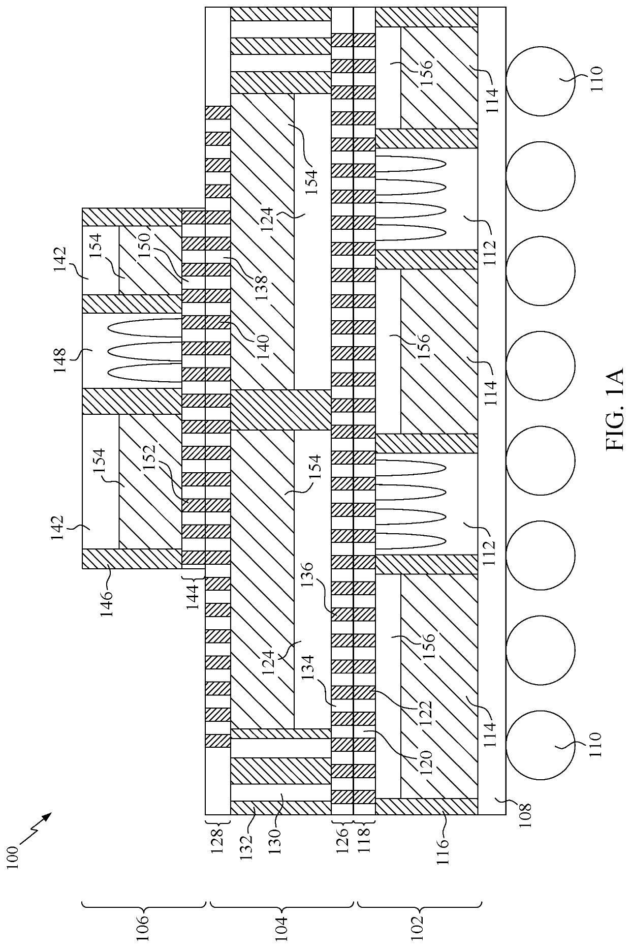
[0051]FIG. 4 is a flow diagram of example operations 400 for fabricating an integrated circuit assembly (e.g., the integrated circuit assembly 100 depicted in FIG. 1), in accordance with certain aspects of the present disclosure. The operations 400 may be performed by an integrated circuit fabrication facility, for example.

[0052]The operations 400 begin, at block 402, where a first reconstituted assembly (e.g., the first reconstituted assembly 102) comprising at least one passive component (e.g., the passive component 112) and a first bonding layer (e.g., the first bonding layer 118) is formed, for example, on a wafer (such as the first wafer 362). At block 404, a second reconstituted assembly (e.g., the second reconstituted assembly 104) comprising one or more first semiconductor dies (e.g., the first dies 124), a second bonding layer (e.g., the second bonding layer 126), and a third bonding layer (e.g., third bonding layer 128) is formed, for example, on a wafer (such as the...


PUM


Abstract

Certain aspects of the present disclosure generally relate to an integrated circuit assembly. One example integrated circuit assembly generally includes a first reconstituted assembly, a second reconstituted assembly, and a third reconstituted assembly. The first reconstituted assembly comprises at least one passive component and a first bonding layer. The second reconstituted assembly is disposed above the first reconstituted assembly and comprises one or more first semiconductor dies, a second bonding layer bonded to the first bonding layer of the first reconstituted assembly, and a third bonding layer. The third reconstituted assembly is disposed above the second reconstituted assembly and comprises one or more second semiconductor dies and a fourth bonding layer bonded to the third bonding layer of the second reconstituted assembly.

Description

BACKGROUNDField of the Disclosure[0001]Certain aspects of the present disclosure generally relate to electronic devices and, more particularly, to an integrated circuit assembly with reconstituted assemblies bonded together through hybrid bonding.Description of Related Art[0002]A continued emphasis in semiconductor technology is to create improved performance semiconductor devices at competitive prices. This emphasis over the years has resulted in extreme miniaturization of semiconductor devices, made possible by continued advances in semiconductor processes and materials in combination with new and sophisticated device designs. Large numbers of transistors are employed in integrated circuits (ICs) in many electronic devices. For example, components such as central processing units (CPUs), graphics processing units (GPUs), and memory systems each employ a large quantity of transistors for logic circuits and memory devices.[0003]In some cases, an IC is powered by a voltage regulator ...

Claims


Application Information

Patent Timeline
IPC IPC(8): H01L23/00H01L23/31H01L23/48H01L21/56
CPCH01L24/29H01L24/27H01L23/3157H01L2924/01014H01L21/565H01L2924/1205H01L2924/14H01L23/481H01L2224/80896H01L23/642H01L25/18H01L25/105H01L2225/1017H01L25/16H01L25/0655H01L2225/1047H01L25/50
Inventor KIM, JONGHAESHAH, MILINDCHIDAMBARAM, PERIANNANLANGARI, ABDOLREZA
Owner QUALCOMM INC
Why Eureka
Try Eureka