Unlock instant, AI-driven research and patent intelligence for your innovation.
Production of Precision Micro-Mask and the AMOLED Display Manufactured Therefrom
Pending Publication Date: 2022-04-28
MAGIC STAR TECHNOLOGY (NINGBO) CO LTD
View PDF0 Cites 0 Cited by
Summary
Abstract
Description
Claims
Application Information
AI Technical Summary
This helps you quickly interpret patents by identifying the three key elements:
Problems solved by technology
Method used
Benefits of technology
Benefits of technology
The patent describes a method for making a precision mask for use in the patterning process of organic light emitting diode (OLED) displays. The method uses a specialized technique to create the mask with high accuracy. This improvement helps ensure the OLED display is patterned correctly, resulting in better quality and performance.
Problems solved by technology
The precision metal masks are key and costly tooling components needed to produce AMOLED display.
Currently, this method can only produce small size FMM.
However, due to the limitations such as compositional uniformity and the mechanical strength of the deposited metal foils produced by electro-forming process, this type of FMM is mostly in research and pilot stage of production.
However, this technology is still in research stage and not yet in production.
Due to the insufficient maturity of the electroforming and hybrid type shadow mask, current mainstream AMOLED display product is limited to the resolution around 500 PPI.
However, in this case the OLED architecture can only use the white OLED plus Color Filter (WOLED+ CF), instead of the Red-Green-Blue Side-By-Side (RGB SBS) architecture.
Moreover, the traditional FMM requires sophisticated precision alignment, tensioning, welding and mounting processes which complicate the production process of AMOLED and increase the cost significantly.
Method used
Image
Click on the blue label to locate the original text in one second.
Reading with bidirectional positioning of images and text.
Examples
example 2-1
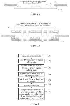
[0105]As shown in FIG. 3, another fabrication method to produce a Precision Micro-Mask (PMM) is provided with current example. The FIG. 3-1˜FIG. 3-7 below provide detailed description of the processing steps to fabricate a PMM and the PMM produced thereof. In current example, the main body of the PMM is composed of the sequentially fabricated debonding layer 20 (in this example the layer 20 represents the debonding layer), the first metal layer 30 and the second metal layer 40.
[0106]As shown in FIG. 3-1, following step S201, select the substrate 10, which maybe semiconductorwafer, siliconwafer, metal substrate, glass or other transparent substrates. Although the substrate 10 maybe either non-transparent or transparent materials, current example uses a non-transparent substrate material. Clean to remove the residual organics or contaminants from the surface of the selected substrate 10, using cleaning agents, ultraviolet (UV) light, and / or plasma.
[0107]As shown in FIG. 3-2, accordi...
example 2-2
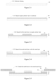
[0113]The difference between the Example 2-2 and Example 2-1 is in the substrate 10 used and the structure of the main body of PMM. The present example uses the transparent substrate, such as glass or other transparent substrate. The main body of the PMM in this case is sequentially fabricate organic polymer layer 20, such as polyimide layer (in current example, the organic polymer layer is indicated as 20 in the Figure); the first metal layer 30, and the second metal layer 40. The thickness of the organic polymer layer 20 is in the range of 0.5˜20 μm.
[0114]The fabrication process include:
S201, select a transparent substrate 10 and clean the surface;
S202, coat the organic polymer layer 20, followed by drying and curing processes;
S203, deposit the first metal layer 30 on the organic polymer layer 20;
S204, coat the second metal layer 40 on the first metal layer 30;
S205, using laser welding to attach the mask frame to the second metal layer along the outer rim of the mask;
S206, remove ...
example 3-1
[0115]As shown in FIG. 4, current example provides another fabrication method to produce a Precision Micro-Mask (PMM). The FIG. 4-1˜FIG. 4-9 below provide detailed description of the processing steps to fabricate a PMM and the PMM produced thereof. In current example, the main body of the PMM is composed of the sequentially fabricated debonding layer 20 (in this example the layer 20 represents the debonding layer), the first metal layer 30 and the second metal layer 40.
[0116]As shown in FIG. 4-1, following step S301, select the substrate 10, which maybe semiconductorwafer, silicon wafer, metal substrate, glass or other transparent substrates. Although the substrate 10 maybe either non-transparent or transparent materials, current example uses a non-transparent substrate material. Clean to remove the residual organics or contaminants from the surface of the selected substrate 10, using cleaning agents, ultraviolet (UV) light, and / or plasma.
[0117]As shown in FIG. 4-2, according to th...
PUM
Property
Measurement
Unit
Length
aaaaa
aaaaa
Length
aaaaa
aaaaa
Length
aaaaa
aaaaa
Abstract
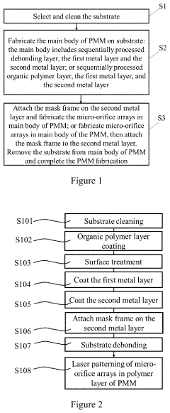
A production method to fabricate precision micro-mask for the production of ultra-high resolution Active-Matrix Organic Light Emitting Diode (AMOLED) display is disclosed. The production process of the micro-mask includes the following processes: S1, select the substrate and cleaning. S2, fabricate the main body of micro-mask on the substrate. The main body of micro-mask includes sequentially preparation of debonding layer, the first metal layer and the second metal layer; or sequentially preparation of organic polymer layer, the first metal layer and the second metal layer. S3, welding the mask frame to the second metal layer after alignment, fabricate perforation through holes in the main body of the micro-mask based on the requirement of the display subpixel design; or fabricate perforation through holes in the micro-mask based on the requirement of the display subpixel design, then welding the mask frame to the second metal of the main body of the micro-mask. The precision micro-mask is completed after debonding from the substrate. With the precision micro-mask prepared, the high efficiency, ultra-high resolution (>1000 ppi) AMOLED display with Red-Green-Blue, or other color combinations, side-by-side architecture can be produced.
Description
TECHNICAL FIELD[0001]A manufacture method of ultrahigh resolution organic optoelectronic device, especially the production of high precision micro-mask and the high-resolution AMOLED display produced therefrom.BACKGROUND ART[0002]AMOLED (Active Matrix Organic Light Emitting Diode Display) is a solid state display device that is composed of organic light emitting diodes based on the stacking of organic semiconductor and other thin films, according to its subpixel and pixel designs. Comparing to the traditional Liquid Crystal Display (LCD), AMOLED possess the advantageous features of light weight, thin form factor, wide viewing angle, good image quality, fast response time, and wider low temperature operating temperature etc., and thus considered the display of the future. By integrating OLED with different Thin Film Transistor (TFT) array driving backplanes, various high end AMOLED display products may be produced in the market, for the applications such as smart phone, television an...
Claims
Application Information
Patent Timeline
Application Date:The date an application was filed.
Publication Date:The date a patent or application was officially published.
First Publication Date:The earliest publication date of a patent with the same application number.
Issue Date:Publication date of the patent grant document.
PCT Entry Date:The Entry date of PCT National Phase.
Estimated Expiry Date:The statutory expiry date of a patent right according to the Patent Law, and it is the longest term of protection that the patent right can achieve without the termination of the patent right due to other reasons(Term extension factor has been taken into account ).
Invalid Date:Actual expiry date is based on effective date or publication date of legal transaction data of invalid patent.


