Organic light emitting diode device and display panel

a technology of organic light and diodes, which is applied in the direction of semiconductor devices, basic electric elements, electrical apparatus, etc., can solve the problems of increasing the complication of mass production processes, unfavorable manufacturing, and the inability of structures to achieve the electric current efficiency and service life level of cascaded tandem structures, so as to solve the insufficiency of service life and blue light efficiency, the effect of improving the service life and service life of side-by-side organic light emi

Pending Publication Date: 2022-06-16
WUHAN CHINA STAR OPTOELECTRONICS SEMICON DISPLAY TECH CO LTD
View PDF1 Cites 0 Cited by
  • Summary
  • Abstract
  • Description
  • Claims
  • Application Information

AI Technical Summary

Benefits of technology

[0008]The present disclosure provides an organic light emitting diode device and a display panel. On one hand, electric current efficiency and service life of the side-by-side organic light emitting diode devices can be improved, solving insufficiency of service life and efficiency of blue light; on the other hand, processes of using a plurality of accurate mask plates to manufacture the multiplied chambers for cascaded tandem organic light emitting diode devices are omitted, thereby reducing manufacturing cost, improving aperture ratio, and facilitating improvement of entire yield.

Problems solved by technology

The structures cannot achieve electric current efficiency and service life level of cascaded tandem structures.
Compared to the SBS device structures, their electric current efficiency can be improved 1.5 to 2 times, and service life can be improved 2 to 4 times. However doubling evaporation chambers is needed for tandem workgroup structures, which increases complication on mass production processes and is unfavorable to manufacturing.
Furthermore, manufacturing processes of the cascaded tandem organic light emitting diode devices are complicated.
Many accurate mask plates are required to be used, resulting in increasement of manufacturing cost, reduction of aperture ratio, and reduction of yield during manufacturing multiplied chambers.

Method used


Image

  • Organic light emitting diode device and display panel
  • Organic light emitting diode device and display panel
  • Organic light emitting diode device and display panel

Examples


Embodiment Construction

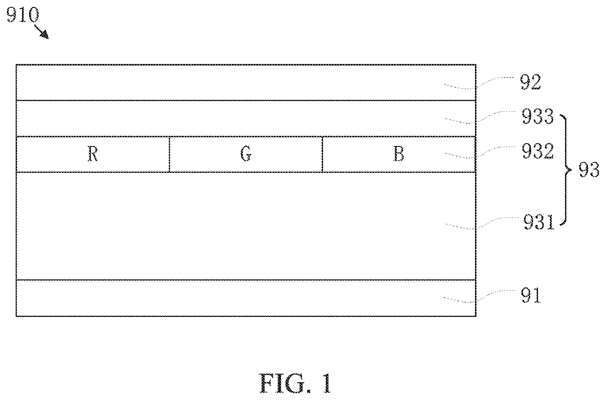
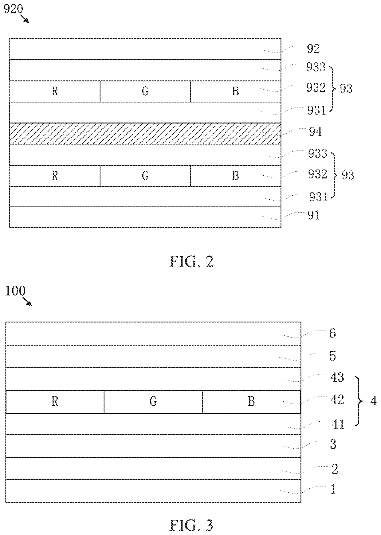
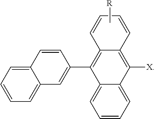
[0025]The technical solutions in the embodiments of the present disclosure are clearly and completely described in the following with reference to the accompanying drawings in the embodiments of the present disclosure. Obviously, the described embodiments are only part of the embodiments of the present disclosure, but are not all embodiments of the present disclosure. All other embodiments obtained by those skilled in the art based on the embodiments of the present disclosure without creative efforts are within the scope of the present disclosure.

[0026]In the description of the present disclosure, unless specified or limited otherwise, terms “mounted,”“connected,”“coupled,” and the like are used in a broad sense, and may include, for example, fixed connections, detachable connections, or integral connections; may also be mechanical or electrical connections or may be communication between each other; may also be direct connections or indirect connections via intervening structures; ...


PUM

PropertyMeasurementUnit
thicknessaaaaaaaaaa
blue light fluorescentaaaaaaaaaa
electric current efficiencyaaaaaaaaaa

Abstract

An organic light emitting diode device and a display panel are provided. The display panel includes the organic light emitting diode device. The organic light emitting diode device includes an emitting material layer. The emitting material layer includes a first common blue-light light-emitting layer, a red-green-blue light emitting layer, and a second common blue-light light-emitting layer.

Description

FIELD OF INVENTION[0001]The present disclosure relates to the field of organic light emitting diodes, and particularly relates to an organic light emitting diode device and a display panel.BACKGROUND OF INVENTION[0002]Currently, technology of active matrix organic light emitting diode (AMOLED) display devices are widely used in mobile phones, and are continuously heading towards directions of low power consumption, low cost, and large dimensions. Compared to liquid crystal displays (LCDs), because organic light emitting diode (OLED) devices can be used in flexible screens, and a problem of short service life on light emitting is improved greatly with development of material technology, mainframe factories and vendors have researched and developed OLED technology one after another. From traditional instrument and center consoles to head up displays (HUDs), streaming rearview mirrors, and illuminations, they are all involved.[0003]Currently, Samsung Electronics Co., Ltd. and LG Corpor...

Claims


Application Information

Patent Timeline
Patent Type & Authority Applications(United States)
IPC IPC(8): H01L51/00
CPCH01L51/0058H01L51/5016H10K59/12H10K50/115H10K50/12H10K50/125H10K50/13H10K85/626H10K85/615H10K50/11H10K71/00H10K2101/10
Inventor LIU, SHENGFANGLI, WEIWEIKIM, MUGYEOM
Owner WUHAN CHINA STAR OPTOELECTRONICS SEMICON DISPLAY TECH CO LTD
Why Eureka
Try Eureka