
Capacitor structure and a chip antenna

a capacitor and chip technology, applied in the direction of solid-state devices, basic electric elements, structural forms of radiating elements, etc., can solve the problems of large tolerances of capacitor capacitance values, poor capacitance value accuracy, and inability to individually select capacitors in mass production, so as to improve capacitance and reactance tolerance of capacitors, reduce losses, and effectual

Active Publication Date: 2022-06-23
COREHW SEMICON OY
View PDF0 Cites 0 Cited by
  • Summary
  • Abstract
  • Description
  • Claims
  • Application Information

AI Technical Summary

Benefits of technology

[0033]The present invention has the advantage that capacitance and reactance tolerance of the capacitor is improved, in other words capacitance values of capacitors are more accurate, losses are reduced, and maximum voltage rating is achieved that fulfills requirements for high power applications. The invented capacitor structure effectively compensates effects of manufacturing tolerances on the capacitance values, thus compensating capacitance variation. Further, capacitance density achieved with the invented capacitor structure enables manufacturing of capacitance values that are particularly useful in chip antennas of mobile wireless devices with physical dimensions that fit well in physical dimensions of other active elements of the antenna.

Problems solved by technology

However, due to manufacturing process variations of this type of semiconductor devices, capacitance value tolerances are large.
In other words, accuracy of the capacitance values achieved is poor, which causes problems in manufacturing devices for certain applications that require accurate capacitor values.
Individual selection of capacitors is not commercially feasible in mass production, but variance of capacitance values in a large mass of capacitor devices needs to be controlled in cost-efficient way.

Method used


Image

  • Capacitor structure and a chip antenna
  • Capacitor structure and a chip antenna
  • Capacitor structure and a chip antenna

Examples


third embodiment

[0093]FIG. 11 is a schematic cross-sectional view of the invented capacitor structure. This structure is based on that of FIG. 6, with T-shape cross section of electrode fingers, but the entire structure has further been mirrored with respect to the metallization layer (504) that forms the lateral part (600b) of one set of the electrode fingers, i.e. arms of T-shapes of one set of electrode fingers.

[0094]In this example, there are pairs of positive electrode fingers that have their superimposed lateral parts (600a), i.e. arms of the T-shapes, on two opposite faces of the capacitor structure and their vertical parts (601a), i.e. stems of the T-shapes pointing in opposite vertical directions towards each other. Between the rows of pairs of positive T-shaped electrode fingers there are negative electrode fingers that have a single lateral part (600b) and two vertical parts (601b) pointing in opposite directions. Lateral part (600b) of the negative electrode finger is partially superimp...

fourth embodiment

[0097]FIG. 12 is a schematic cross-sectional view of the invented capacitor structure. This structure is based on that of FIG. 9, with inverted L-shape cross section of electrode fingers, but the entire structure has further been mirrored with respect to the metallization layer (504) that forms the lateral part (600b) of one set of the electrode fingers, i.e. legs of L-shapes of one set of electrode fingers.

[0098]In this example, each positive electrode finger has two superimposed lateral parts (600a), i.e. legs of the L-shapes, on two opposite faces of the capacitor structure and a vertical part (601a) coupling the two lateral parts (600a) together. Negative electrode fingers have a single lateral part (600b) and two vertical parts (601b) pointing in opposite directions. Lateral part (600b) of the negative electrode finger is partially superimposed with the lateral parts (600a) of the adjacent positive electrode finger.

[0099]This kind of structure may be beneficial, if there is a h...


PUM

PropertyMeasurementUnit
electrically conductingaaaaaaaaaa
vertical distanceaaaaaaaaaa
widthaaaaaaaaaa

Abstract

A capacitor structure implemented using a semiconductor process. The capacitor structure includes a plurality of interdigitated positive and negative electrode fingers separated by a dielectric material, and a plurality of patterned metallization layers separated by the dielectric material. Each interdigitated electrode finger comprises a lateral part formed on one of at least two essentially parallel first metallization layers and a vertical part includes a plurality of superimposed slabs or bars disposed on a plurality of second metallization layers between said first metallization layers and electrically connected to each other and to the lateral part with a plurality of electrically conducting vias traversing through dielectric material separating adjacent metallization layers. Vertical distance between each pair of at least partially superimposed lateral parts of two adjacent electrode fingers is substantially equal to lateral distance between two adjacent vertical parts.

Description

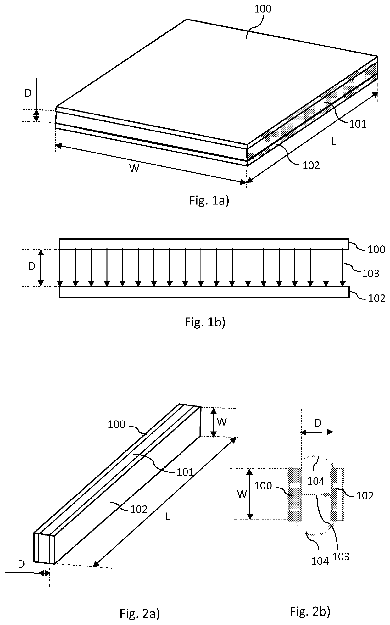
CROSS-REFERENCE TO RELATED APPLICATIONS[0001]This application is a continuation of PCT International Application No. PCT / FI2019 / 050513 filed Jun. 28, 2019, the disclosure of this application is expressly incorporated herein by reference in its entirety.FIELD[0002]The present invention relates to a semiconductor device structure, in particular to a capacitor structure. More particularly, the present invention discloses a chip antenna implemented by a semiconductor process.BACKGROUND[0003]FIG. 1a shows a parallel plate capacitor with conductor plate length L, conductor plate width W and distance between two plates (100, 102) is D. A gap between the first conductor plate (100) and the second conductor plate (102) is filled with dielectric medium (101) having thickness D and relative permittivity of ∈r and ∈0 is constant for permittivity of vacuum. Capacitance of the parallel plate capacitor is given by equation:C=∈0×∈r×(W×L) / D  (1)[0004]In semiconductor industry, when insulator is used...

Claims


Application Information

Patent Timeline
Patent Type & Authority Applications(United States)
IPC IPC(8): H01Q1/22H01L23/66H01L49/02H01L23/522H01Q1/38
CPCH01Q1/2283H01L23/66H01L28/90H01L2223/6677H01L23/5226H01Q1/38H01L23/5223H01L28/40H01L28/86H01L28/88H01L28/91
Inventor HAKAMO, MARKUSTAKALO, TOMI-PEKKAKOTILAINEN, PETRIHELIÖ, PETRI
Owner COREHW SEMICON OY
Learn More