
Optical Multi/Demultiprexing Circuit

a multi-prexing circuit and optical technology, applied in the field of optical wavelength multi-prexing circuits, can solve the problems of increasing loss, increasing variation (ripple) of transmission loss, and difficulty in achieving stable manufacturing

Active Publication Date: 2022-08-25
NIPPON TELEGRAPH & TELEPHONE CORP
View PDF4 Cites 0 Cited by
  • Summary
  • Abstract
  • Description
  • Claims
  • Application Information

AI Technical Summary

Benefits of technology

The present invention provides a synchronized AWG-type optical wavelength multi / demultiplexing circuit with a high rectangular transmission loss spectrum that is able to secure loss flatness of the transmission band, maintain / reduce the guard bandwidth of wavelength channel spacing, and broaden the transmission bandwidth. The invention also provides an asymmetric Mach-Zehnder interferometer that can reproduce high repetition frequency characteristics and adjust the light intensity minimum point to the center wavelength. The transfer matrix elements of the invention have constant phase characteristics, which are sufficient compared to the transmission signal. The invention can maintain / reduce the guard bandwidth and broaden the transmission bandwidth while also securing phase flatness.

Problems solved by technology

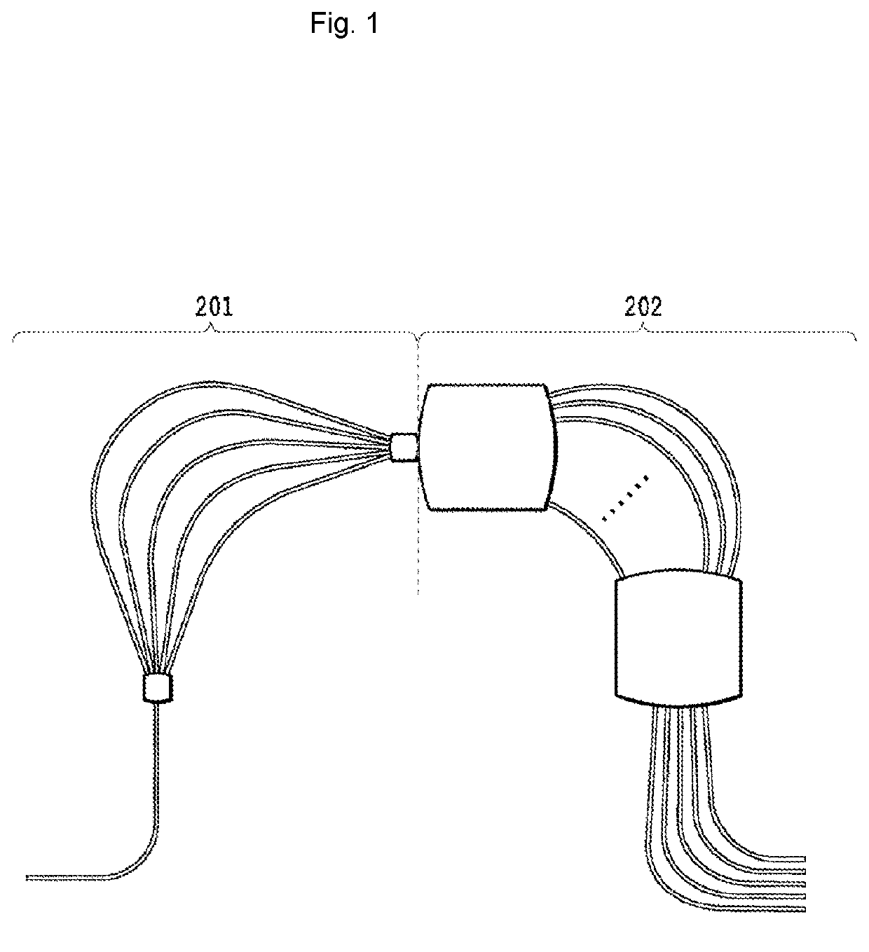
Since loss per AWG is constant, however, loss tends to increase in synchronized AWGs constituted by connecting two AWGs in series.
Furthermore, when constituting a field modulation device requiring highly repetitive cyclicity with an AWG, the difficulty of achieving stable manufacturing is an issue.
As a result, a shortcoming of synchronized AWGs of a type that use waveguides running parallel to each other for the connecting portion with the downstream AWG is that broadening the transmission band will lead to issues such as increased variation (ripple) of transmission loss and increased loss variation in the transmission band.
Considering this point, in a parallel waveguide connection-type synchronized AWG in which the combined field shape departs from a Gaussian distribution by a large degree, the problem of increased transmission loss occurs, and the problem of increased loss variation occurs in the case where the degree of departure from a Gaussian distribution varies.
However, with this method, there is a problem in that the transition region width between the transmission region and the cutoff region also increases, resulting in an increase in the wavelength region that cannot be used for transmission.
Additionally, as disclosed in NPL 2, with parallel waveguides, there is also the problem of wavelength dispersion occurring due to supermodes being generated for waveguide coupling.
However, there is a problem in that the phase spectrum of the synchronized AWG disclosed in NPL 3 cannot be flattened with a synchronized AWG alone, resulting in group delay variation of approximately 5 ps.
In such a case, a problem arises in that phase variation and loss variation in the transmission band occur, and, furthermore, crosstalk variation occurs even in the cutoff region.
However, in order to broaden the transmission region bandwidth further with existing synchronized AWGs, there are various restrictions and problems such as will be described below depending on the type of synchronized AWG.
That is, with a technique that also uses an AWG for the field modulation device, there is the problem of increased loss.
Also, with a configuration that increases the number of parallel waveguides of the connecting part between the field modulation device and the downstream AWG, there is the problem of it being difficult to further suppress both the amount of loss variation in the transmission region and the width of the cutoff region between wavelength channels.
Additionally, there is also the problem of wavelength dispersion occurring due to supermodes resulting from mode coupling between waveguides of a parallel waveguide unit.
There are also problems with a configuration in which a multimode waveguide is used for the connecting part between the field modulation device and the downstream AWG, and input signal light is branched and then guided to two input ports of the mode converter / multiplexer after providing a predetermined delay difference.
In this case, there is the problem of large wavelength dispersion occurring when further broadening the transmission bandwidth.
Furthermore, with a synchronous AWG that uses an MMI-Phaser as the field modulation device, there is concern about the occurrence of phase variation and loss variation in the transmission band.

Method used


Image

  • Optical Multi/Demultiprexing Circuit
  • Optical Multi/Demultiprexing Circuit
  • Optical Multi/Demultiprexing Circuit

Examples


embodiment 1

[0109]FIG. 17 is a schematic view showing the basic configuration of an optical wavelength multi / demultiplexing circuit 10A according to embodiment 1 of the present invention.

[0110]As shown in FIG. 17, the optical wavelength multi / demultiplexing circuit 10A according to embodiment 1 of the present invention is constituted by coupling an AWG (Arrayed Waveguide Grating) 102 designed with wavelength channel spacing of 100 GHz and a field modulation device 101 having an optical frequency repetition period (FSR) of 100 GHz.

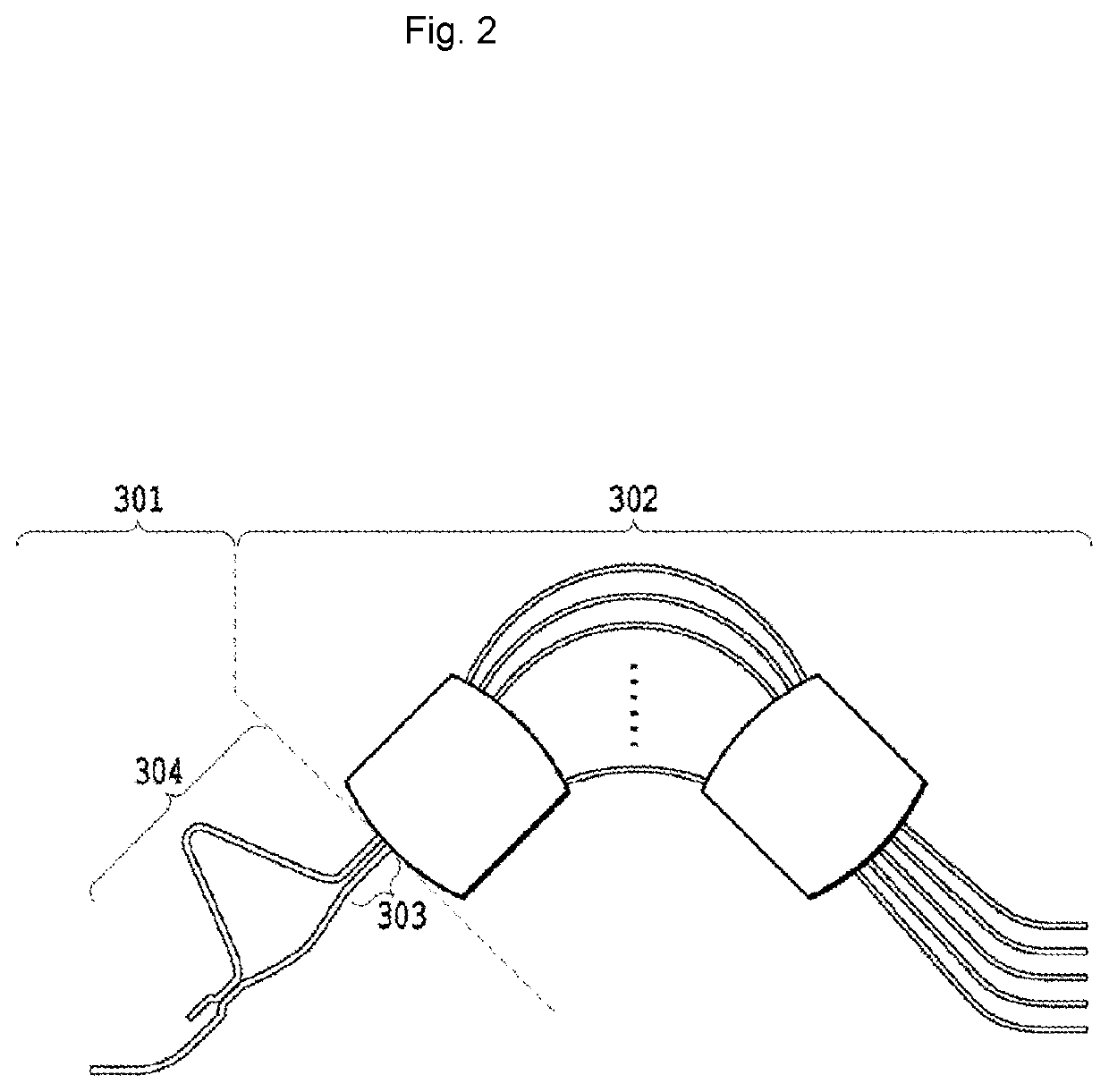
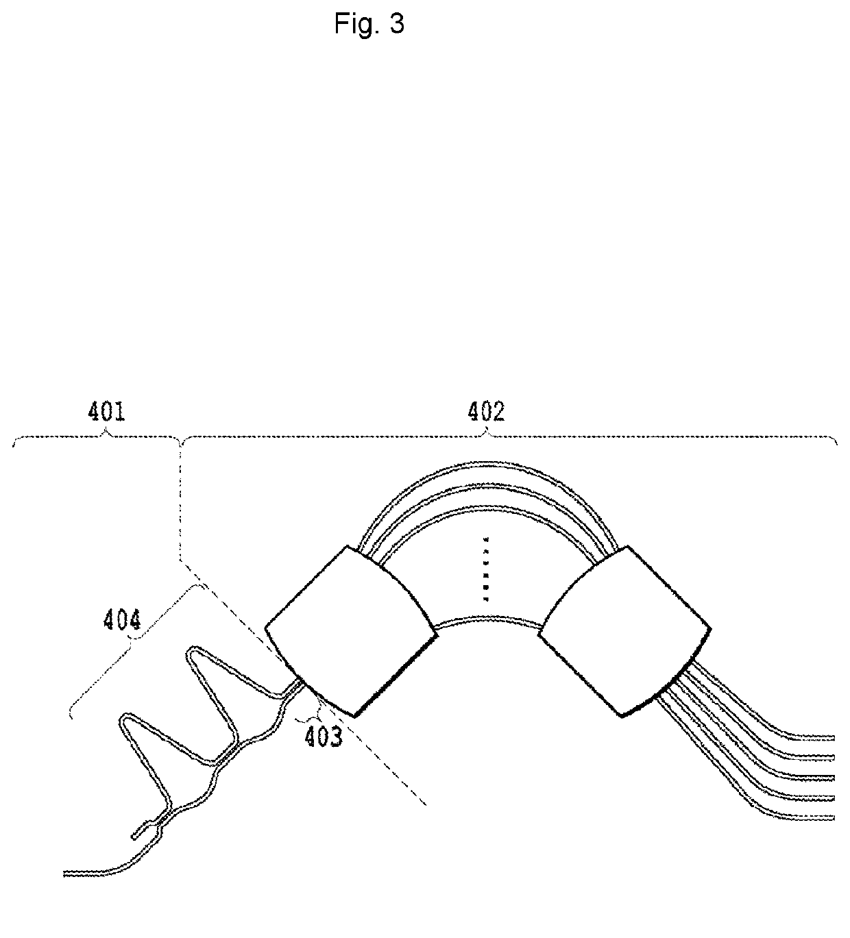
[0111]Of these, the field modulation device 101 is constituted by a common input waveguide 103, an optical branching unit 108, four optical delay lines 104, 105, 106 and 107, a multiplex interference unit 112, and a mode converter / multiplexer 115. Also, the optical branching unit 108 is constituted by a first optical branching element 109 with a branching ratio of 12%, a second optical branching element 110 with a branching ratio of 70%, and a third optical branching e...

embodiment 2

[0124]FIG. 20 is a schematic view showing the basic configuration of an optical wavelength multi / demultiplexing circuit 10B according to embodiment 2 of the present invention.

[0125]As shown in FIG. 20, the optical wavelength multi / demultiplexing circuit 10B according to embodiment 2 of the present invention is constituted by coupling an AWG (Arrayed Waveguide Grating) 2602 designed with wavelength channel spacing of 100 GHz and a field modulation device 2601 having an optical frequency repetition period (FSR) of 100 GHz.

[0126]Of these, the field modulation device 2601 is constituted by a common input waveguide 2603, an optical branching element 2608, four optical delay lines 2604, 2605, 2606 and 2607, a multiplex interference unit 2612, and a mode converter / multiplexer 2615. The optical branching unit 2608 is constituted by a first optical branching element 2609 with a branching ratio of 15% and a second optical branching element 2610 and a third optical branching element 2611 with ...

embodiment 3

[0142]FIG. 24 is a schematic view showing the basic configuration of an optical wavelength multi / demultiplexing circuit 10C according to embodiment 3 of the present invention.

[0143]Referring to FIG. 24, the optical wavelength multi / demultiplexing circuit 10C according to embodiment 3 of the present invention is constituted by coupling an AWG (Arrayed Waveguide Grating) 2902 designed with wavelength channel spacing of 200 GHz and a field modulation device 2901 having an optical frequency repetition period (FSR) of 200 GHz.

[0144]Of these, the field modulation device 2901 is constituted to include a common input waveguide 2903, an optical branching unit 2909, and five optical delay lines 2904, 2905, 2906, 2907 and 2908. Also, the field modulation device 2901 includes a multiplex interference unit 2914 and a mode converter / multiplexer 2917. The optical branching unit 2909 is constituted by a first optical branching element 2910 with a branching ratio of 46%, a second optical branching e...


PUM


Abstract

Provided is an optical wavelength multi / demultiplexing circuit with a high rectangular transmission loss spectrum that is able to secure loss flatness of a transmission band, maintain / reduce a guard bandwidth of wavelength channel spacing, and broaden a transmission bandwidth. The circuit uses a multimode waveguide for a connecting part between a field modulation device and an AWG. The field modulation device is constituted by a common input waveguide, an optical branching unit, optical delay lines, a multiplex interference unit, and a mode converter / multiplexer.

Description

TECHNICAL FIELD[0001]The present invention relates to an optical wavelength multi / demultiplexing circuit that uses an Arrayed Waveguide Grating (hereinafter, AWG) and has a wide transmission bandwidth.BACKGROUND ART[0002]Conventionally, network systems that connect multiple points utilizing a ring network, a mesh network or the like, and that flexibly switch communication channels have been built, following advances in optical fiber communication systems. In such advanced networks, it is sought to process optical signals directly through multiple points, without converting the optical signals into electrical signals. Optical wavelength multi / demultiplexing circuits used here are required to have a broad and flat transmission band and low loss transmission characteristics.[0003]Also, due to the rapid increase in traffic of data centers, mobile networks and the like in recent years, increasing the speed and capacity of optical trunk line networks that support these data centers and th...

Claims


Application Information

Patent Timeline
Patent Type & Authority Applications(United States)
IPC IPC(8): G02B6/12G02B6/293
CPCG02B6/12011G02B6/12016G02B6/29361G02B2006/12159G02B6/12019G02B6/29358
Inventor OGUMA, MANABUMORIWAKI, OSAMUSUZUKI, KENYA
Owner NIPPON TELEGRAPH & TELEPHONE CORP
Learn More