Three-dimensional stacked phase change memory and preparation method thereof
a phase change memory and three-dimensional stack technology, applied in the field of microelectronic devices and memories, can solve the problems of slow read and write speed, inability to repeat erasing and writing fewer times, and difficulties in conventional dram technology in many aspects, so as to achieve small operating current, increase process cost, and increase the effect of uneven surfa
- Summary
- Abstract
- Description
- Claims
- Application Information
AI Technical Summary
Benefits of technology
Problems solved by technology
Method used
Image

Examples
embodiment 1
[0054]This embodiment includes the following steps.
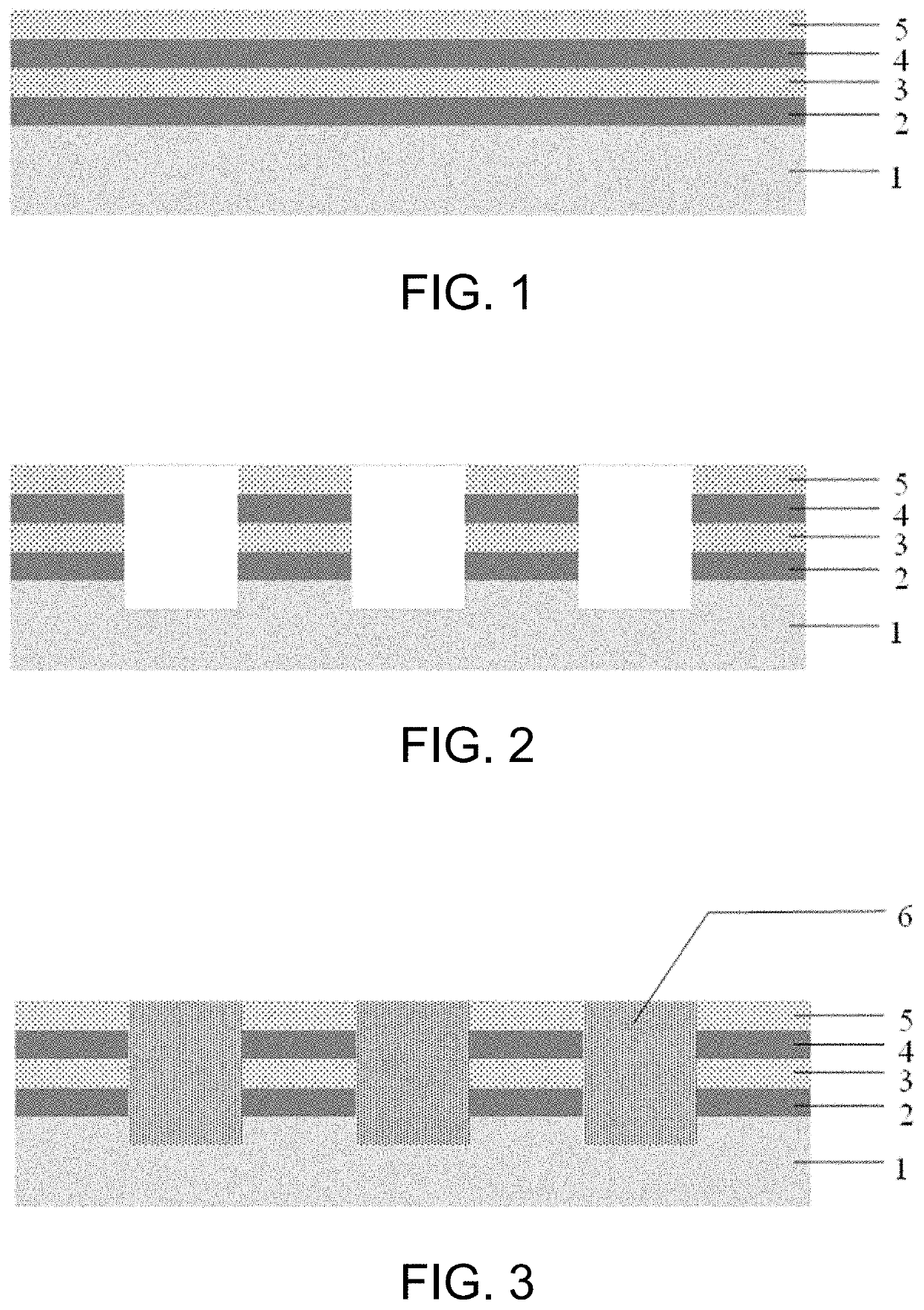
[0055]Step 1: On the single crystal silicon substrate 1 with a SiO2 insulating layer on its surface, 100 nm of Al is deposited as the first electrode layer 2 through an electron beam evaporation process.
[0056]Step 2: On the basis of Step 1, PECVD is performed to deposit 100 nm of SiO2 as the first insulating layer 3 and the first electrode pin layer is exposed.
[0057]Step 3: On the basis of Step 2, 100 nm of Al is deposited as the second electrode layer 4 through electron beam evaporation, which is completely located on the first insulating layer.
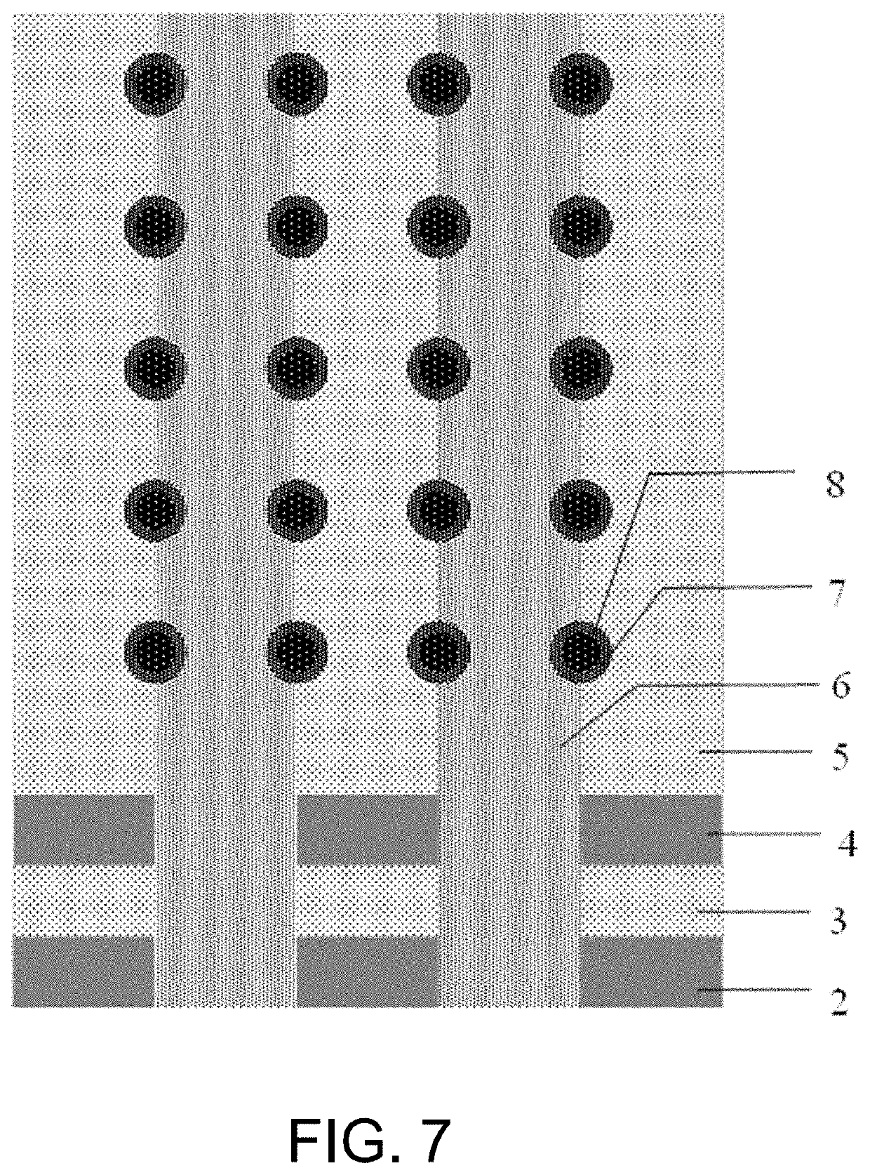
[0058]Step 4: On the basis of Step 3, PECVD is performed to grow 100 nm of SiO2 as the second insulating layer 5 and the second electrode pin layer is exposed (as shown in FIG. 1; FIG. 1 does not show the exposed pins. For details on the exposed pins, please refer to FIG. 7).
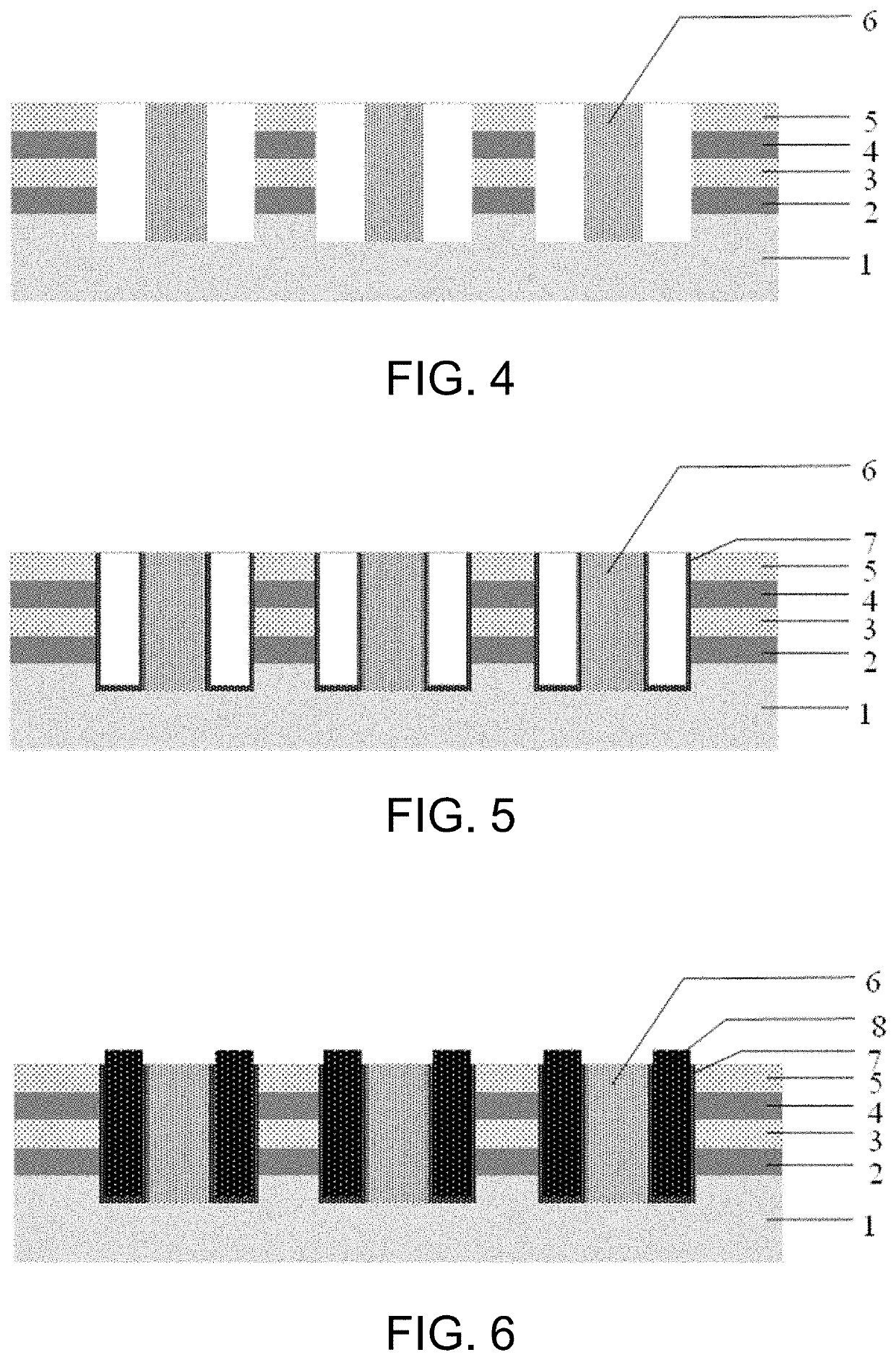
[0059]Step 5: The above steps are repeated to prepare more stacked layers.
[0060]Step 6: The ICP etching equipment is u...
PUM
| Property | Measurement | Unit |
|---|---|---|
| projection length | aaaaa | aaaaa |
| electrical | aaaaa | aaaaa |
| thermal isolation | aaaaa | aaaaa |
Abstract
Description
Claims
Application Information
 - R&D
- Intellectual Property
- Life Sciences
- Materials
- Tech Scout
- Unparalleled Data Quality
- Higher Quality Content
- 60% Fewer Hallucinations
Browse by: Latest US Patents, China's latest patents, Technical Efficacy Thesaurus, Application Domain, Technology Topic, Popular Technical Reports.
© 2025 PatSnap. All rights reserved.Legal|Privacy policy|Modern Slavery Act Transparency Statement|Sitemap|About US| Contact US: help@patsnap.com